Open Nav

To ensure peak performance, rigorous Hdi Pcb Design & Testing protocols are implemented alongside strategic HDI PCB Thermal Management to effectively dissipate heat in compact spaces. This meticulous engineering guarantees exceptional Hdi Pcb Reliability, making it ideal for mission-critical applications. Furthermore, dedicated Hdi Pcb Faq & Support resources provide expert guidance throughout the development process. By combining these elements, a High Density Interconnect PCB delivers the power, efficiency, and durability required for today's most sophisticated electronic devices.
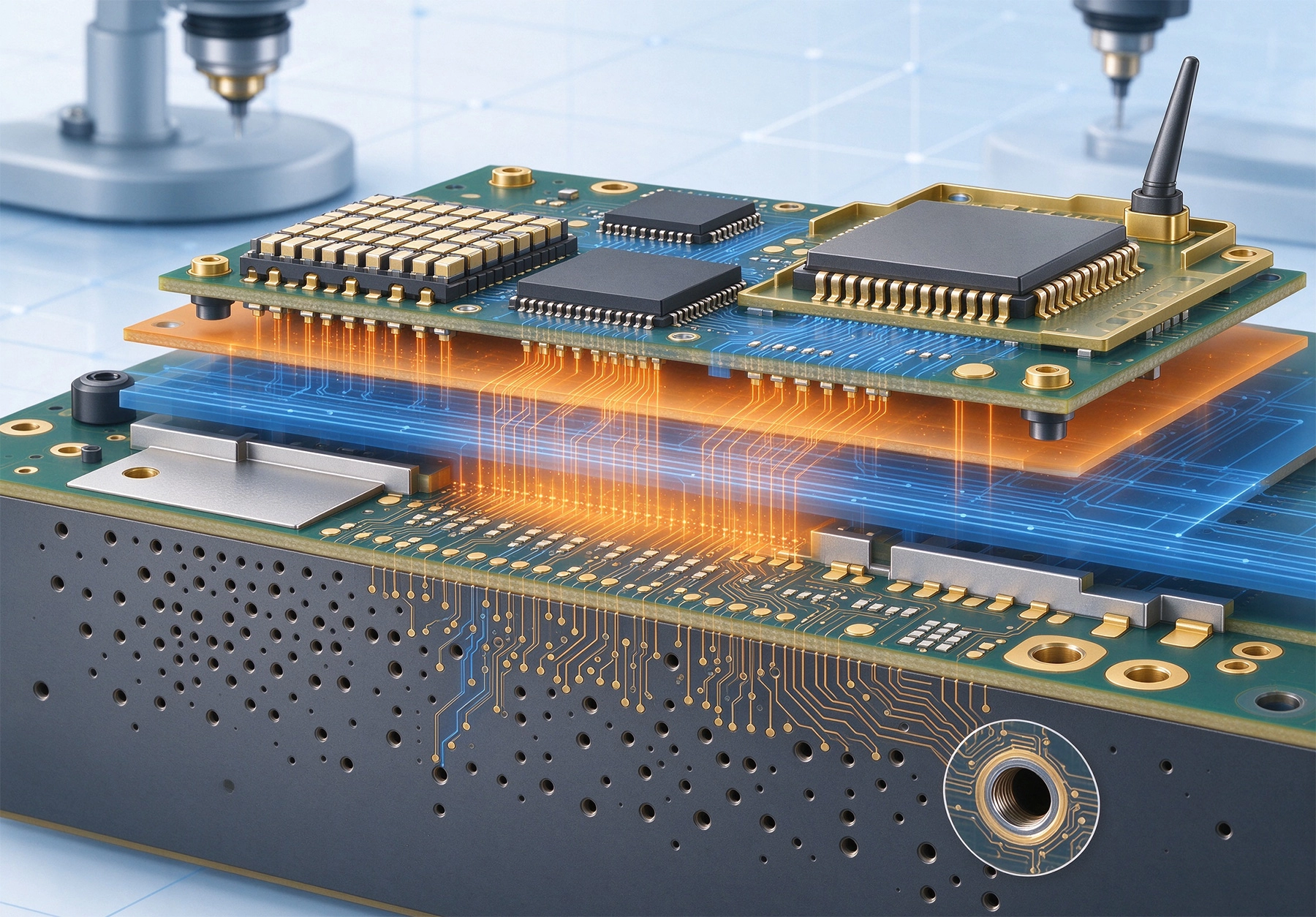
The Impact of HDI on LiDAR and Radar Sensor PerformanceOctober/15/2026Autonomous driving and advanced driver-assistance systems (ADAS) rely on a continuous stream of high-fidelity sensor data. LiDAR and radar are the two primary perception technologies enabling vehicles to "see" their surroundings, but their performance is only as good as the printed circuit boards ...
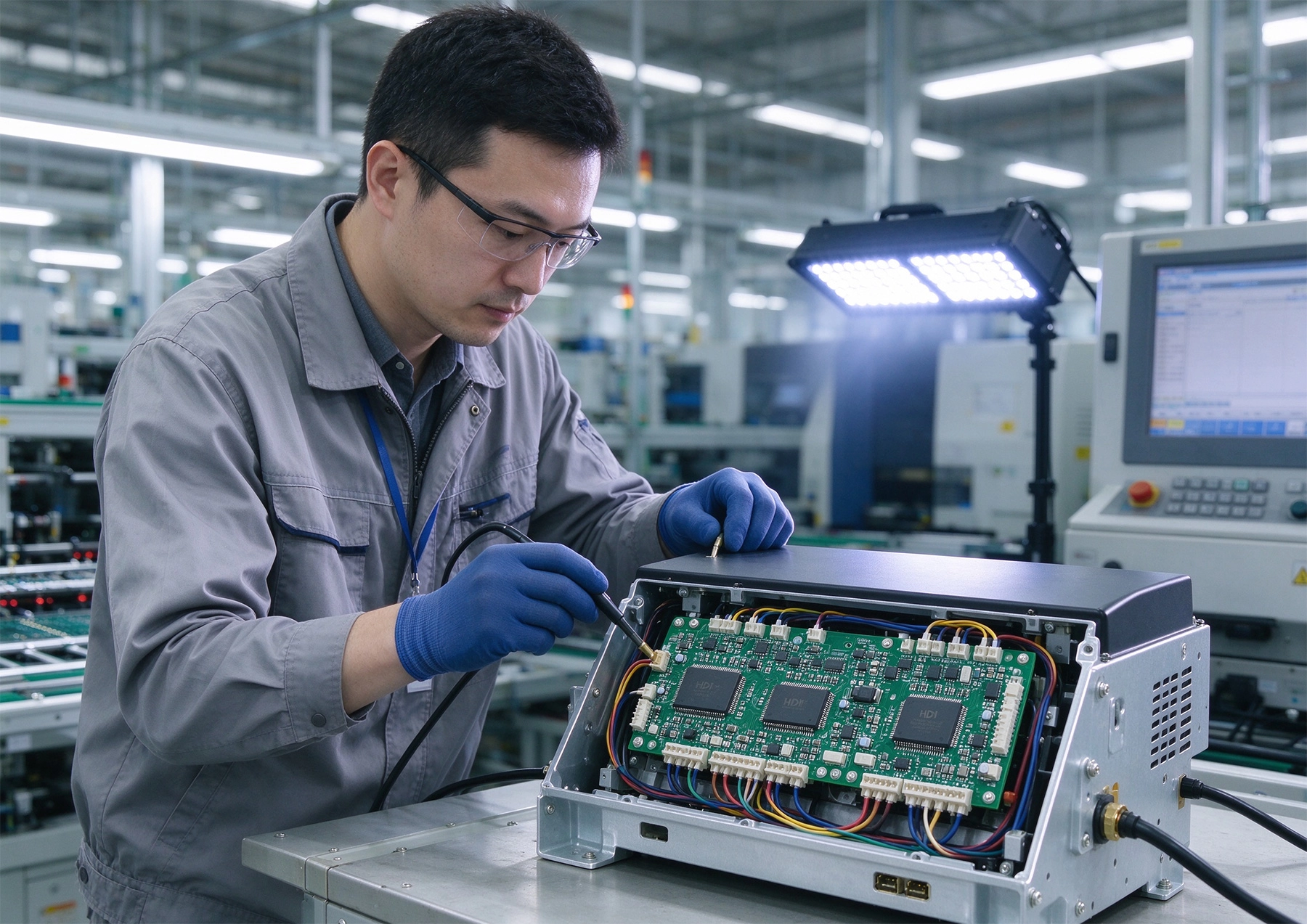
Using HDI Technology in Solar Inverters and ConvertersOctober/14/2026Solar inverters and converters are undergoing a significant transformation. As photovoltaic systems become more powerful, more compact, and more intelligent, the printed circuit boards inside them must handle higher switching frequencies, tighter thermal management, and greater functional density....
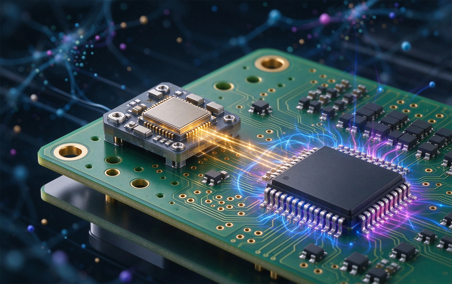
Why IoT Sensors Rely on High-Density Interconnect TechnologyOctober/13/2026Modern IoT sensors are no longer simple devices that read temperature, pressure, or motion and send data through a basic interface. Today’s sensors combine analog front ends, microcontrollers, wireless modules, power management, MEMS structures, and sometimes edge AI processing in extremely small ...
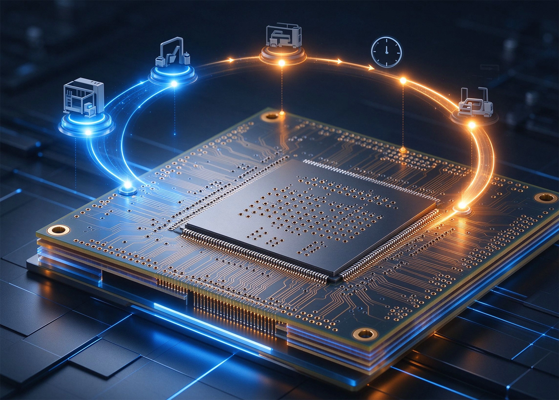
What is the Lead Time for Manufacturing Custom HDI Boards?October/12/2026High-Density Interconnect (HDI) printed circuit boards represent the cutting edge of PCB manufacturing, enabling finer trace widths, smaller vias, and higher component densities than conventional multilayer boards. But with this complexity comes a critical question for every engineer and procureme...
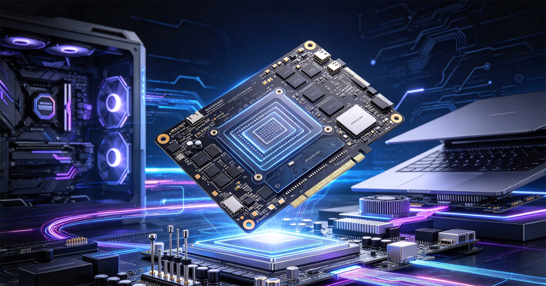
HDI Solutions for High-Performance Gaming Consoles and LaptopsOctober/10/2026Modern gaming consoles and laptops are pushing hardware limits harder than ever. Faster GPUs, higher memory bandwidth, PCIe 5.0 interfaces, and compact thermal designs all demand more from the printed circuit board. That is why HDI solutions for high-performance gaming consoles and laptops have be...
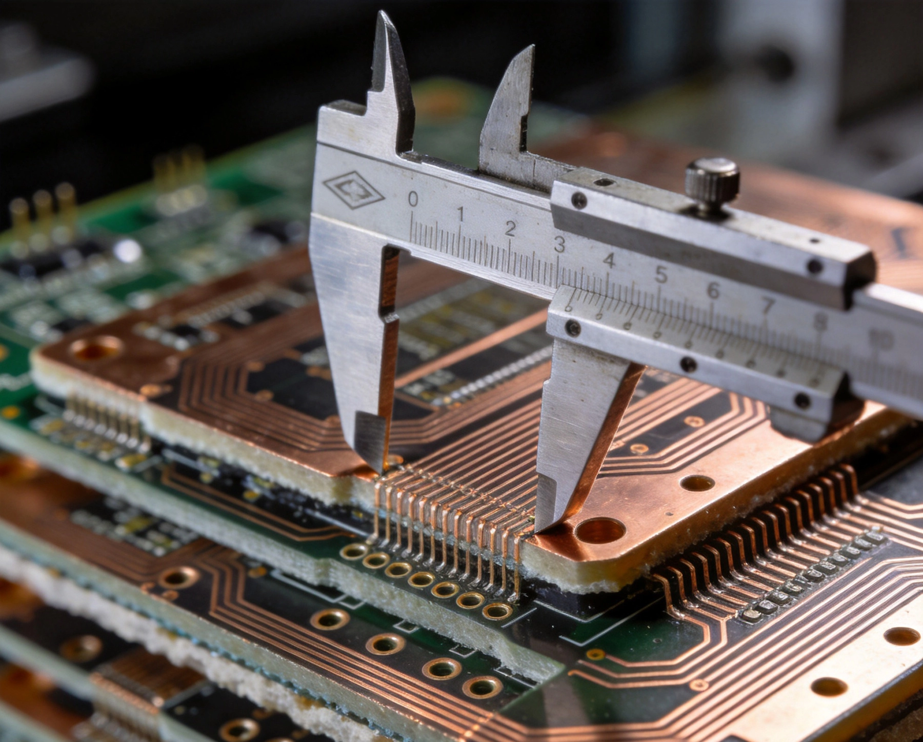
Managing Layer-to-Layer Registration Accuracy in Multilayer HDIOctober/09/2026Registration accuracy—the alignment between layers in a multilayer PCB—doesn't get much attention until it causes problems. And in HDI designs, it causes problems more often than in conventional multilayer boards. The combination of fine features, microvias, and sequential lamination creates align...
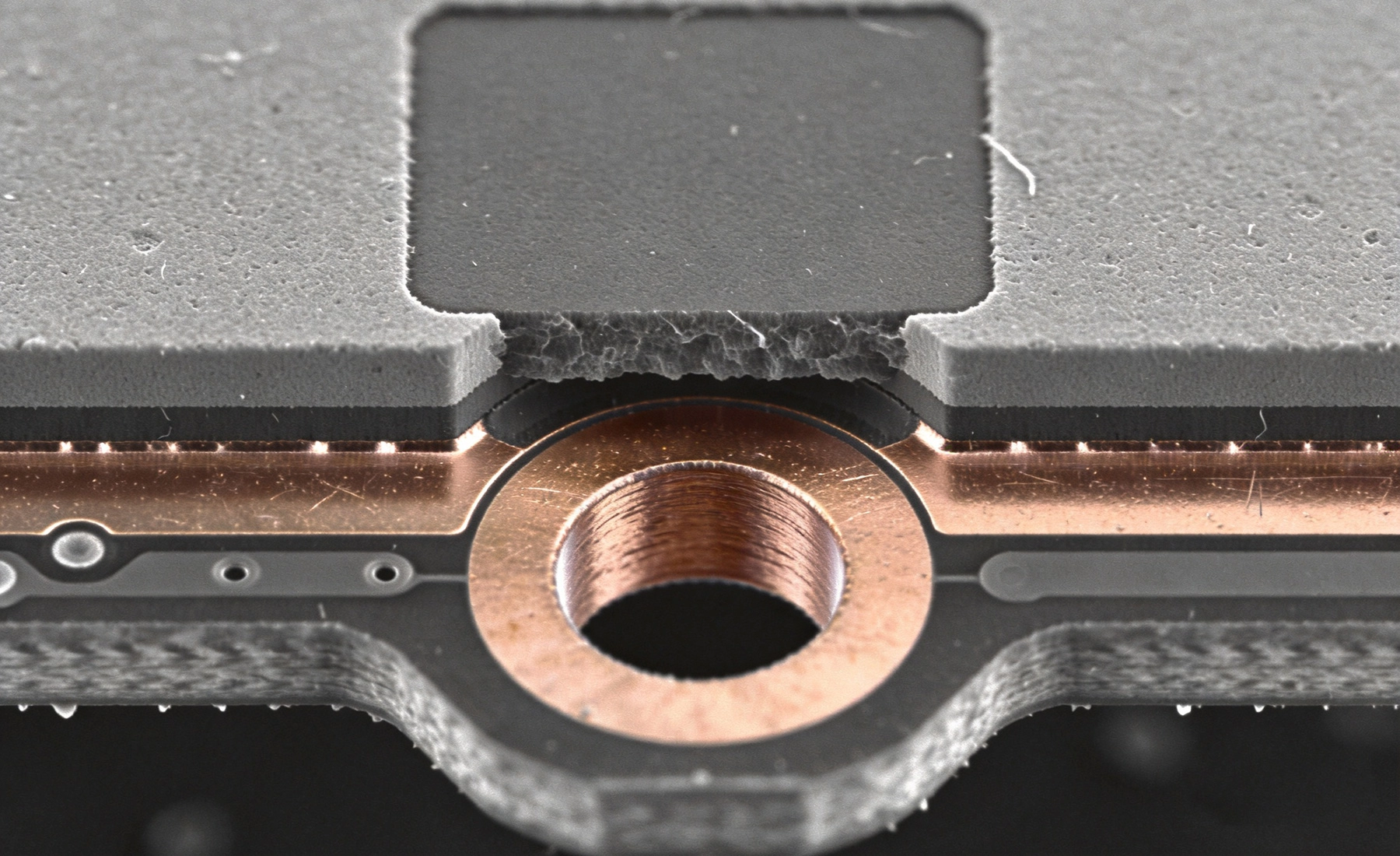
Reliability Challenges of Via-in-Pad Plating Filled (VIPPO) TechnologySeptember/30/2026Via-in-pad is one of those design techniques that looks deceptively simple on a schematic but carries substantial manufacturing complexity underneath. The concept is straightforward: drill a hole at a component pad location, plate it to form an electrical connection to an internal layer, fill it w...
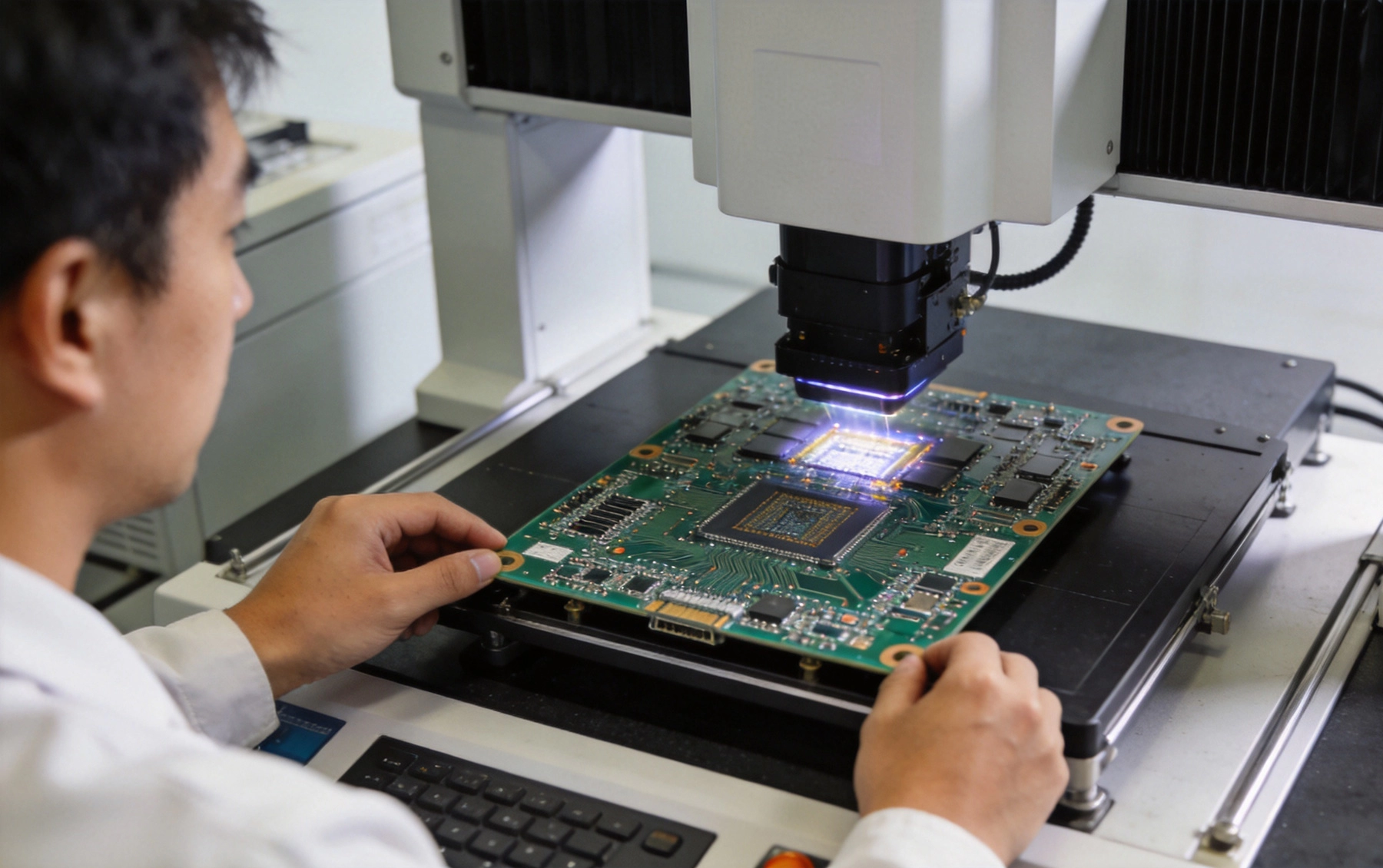
Non-Destructive Testing Techniques for Multilayer HDI PCBsSeptember/29/2026Multilayer High-Density Interconnect (HDI) PCBs form the foundation of modern compact, high-performance electronics including smartphones, medical implants, aerospace systems, and automotive advanced driver assistance systems. With trace widths as small as 25μm, microvias (blind, buried, and stack...
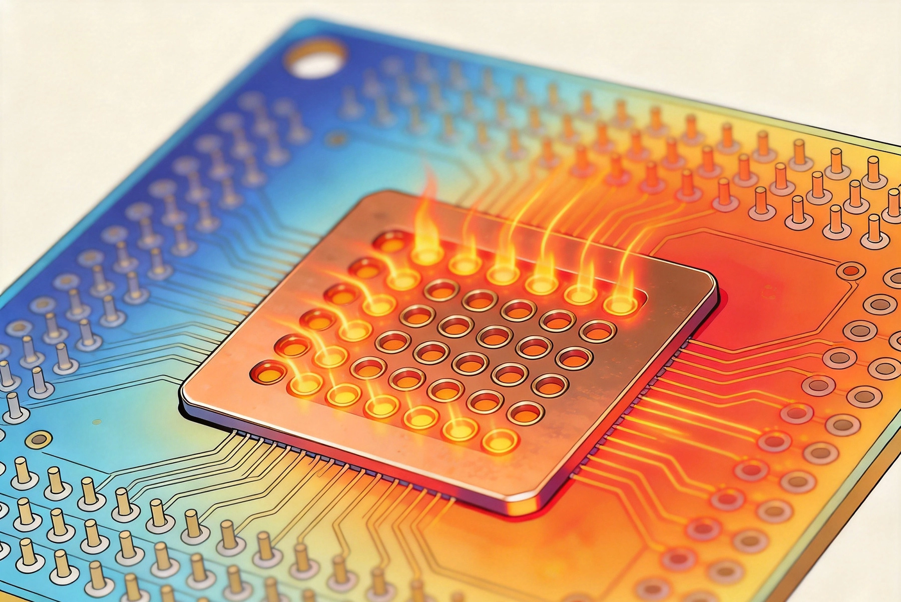
The Impact of Via-in-Pad on Thermal Performance and ReliabilitySeptember/26/2026Via-in-pad — placing a via directly within a component land pad rather than beside it — is one of the most consequential design decisions in modern PCB layout. It affects thermal performance, solder joint integrity, manufacturing cost, and long-term reliability in ways that are not always obvious ...
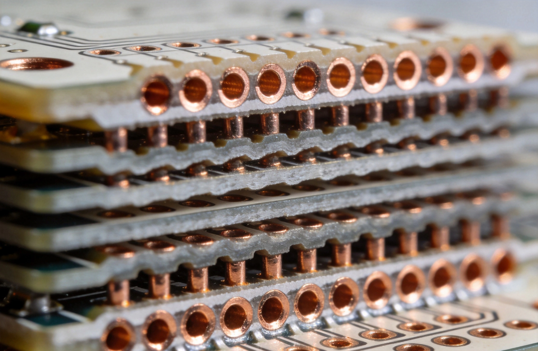
The Art of Microvia Placement: Staggered vs. Stacked ViasSeptember/24/2026As electronics continue their relentless march toward miniaturization, high-density interconnect (HDI) technology has become standard practice rather than exotic exception. And at the heart of every HDI design lies the microvia—those laser-drilled, small-diameter vias that make the interlayer conn...
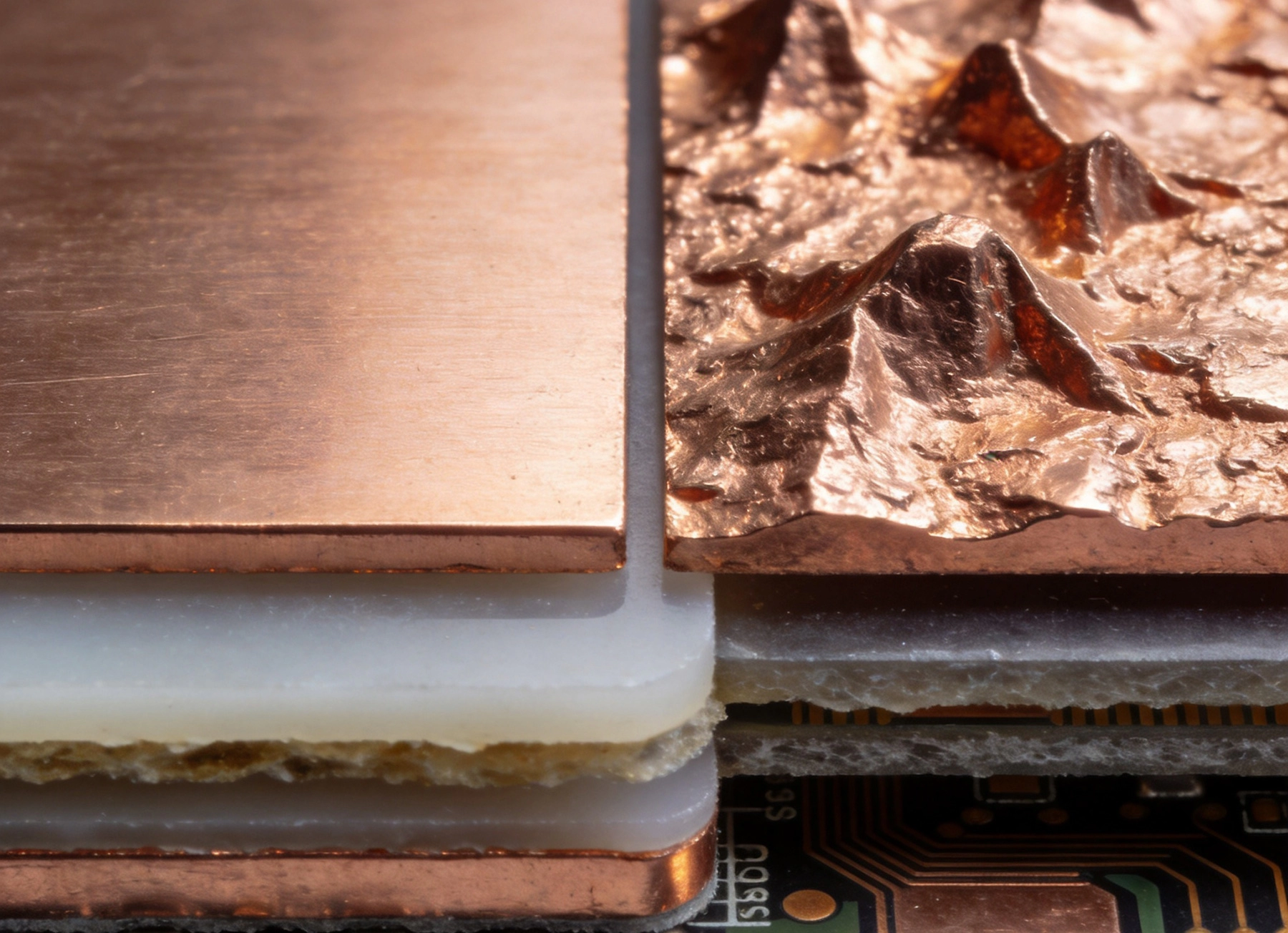
Understanding the Role of Copper Foil Roughness in Signal IntegritySeptember/23/2026Signal integrity engineers spend considerable effort on trace geometry, impedance control, and crosstalk management. Yet one factor often receives insufficient attention until problems emerge in production or field operation: copper foil surface roughness. At low frequencies, the microscopic textu...
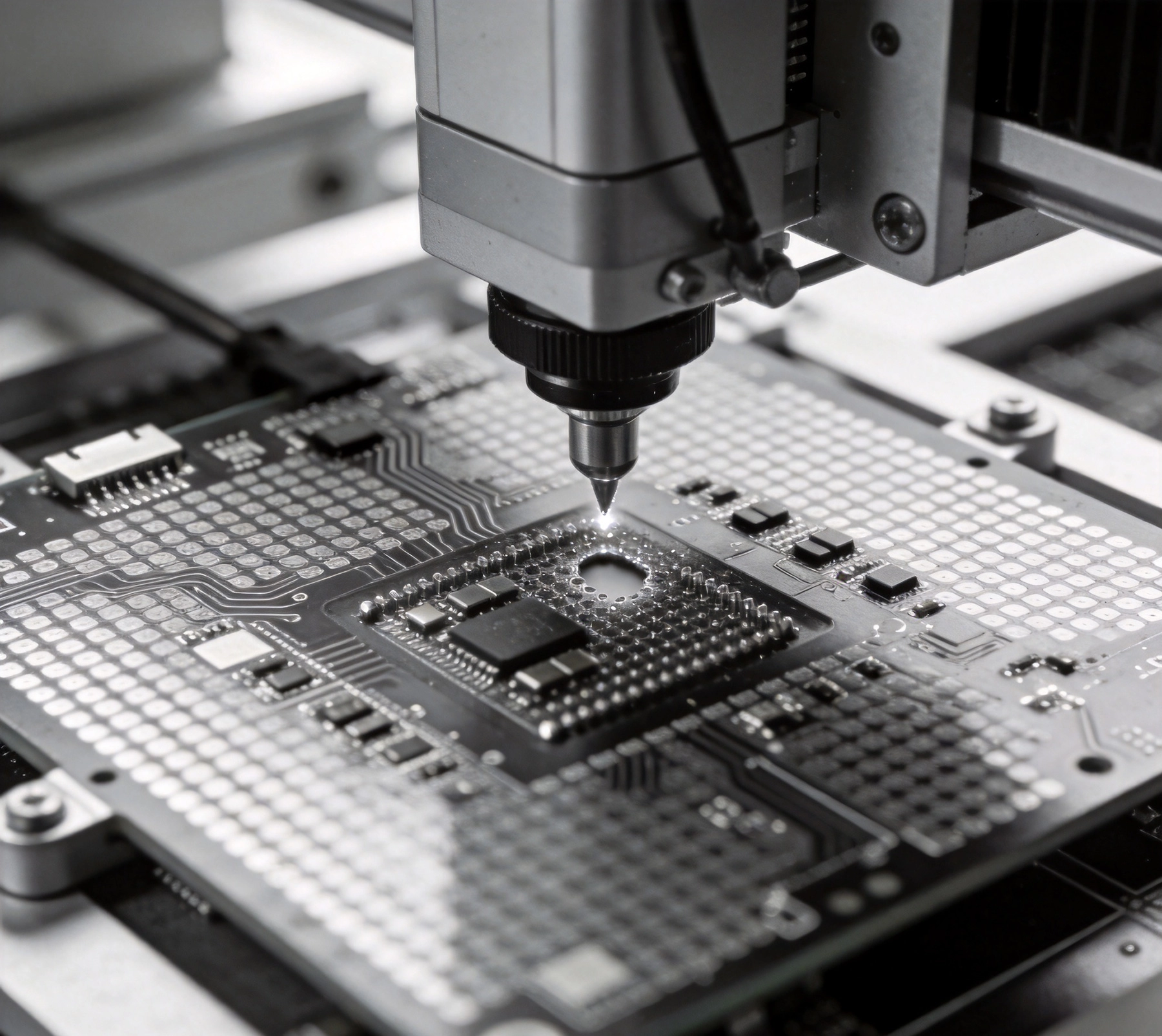
Overcoming Common Manufacturing Defects in High-Density InterconnectsSeptember/21/2026 High-density interconnect (HDI) PCBs have transformed electronics manufacturing by enabling dramatically smaller, lighter, and more capable devices. From smartphones to medical implants, HDI technology makes possible what was impossible with traditional board designs. Yet this miniaturization co...
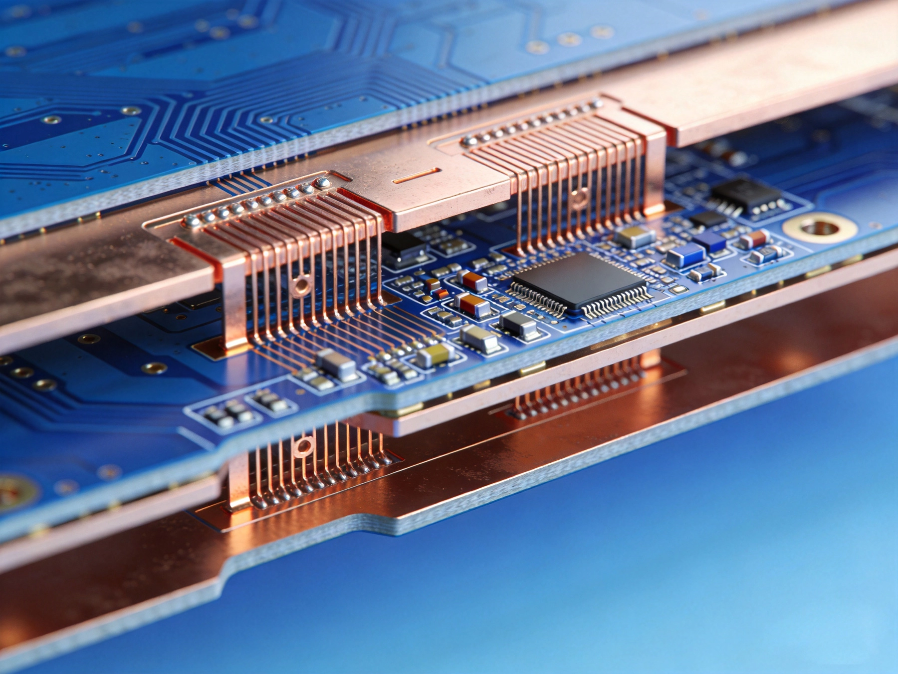
How HDI Technology Enables the Miniaturization of Modern ElectronicsSeptember/20/2026Open any smartphone, peel back the EMI shield, and look at the main PCB. What you see is a board roughly the size of a credit card carrying an application processor with 2,000+ solder balls on 0.35 mm pitch, 8–16 GB of LPDDR memory in a package-on-package stack, a mmWave antenna module, hundreds o...
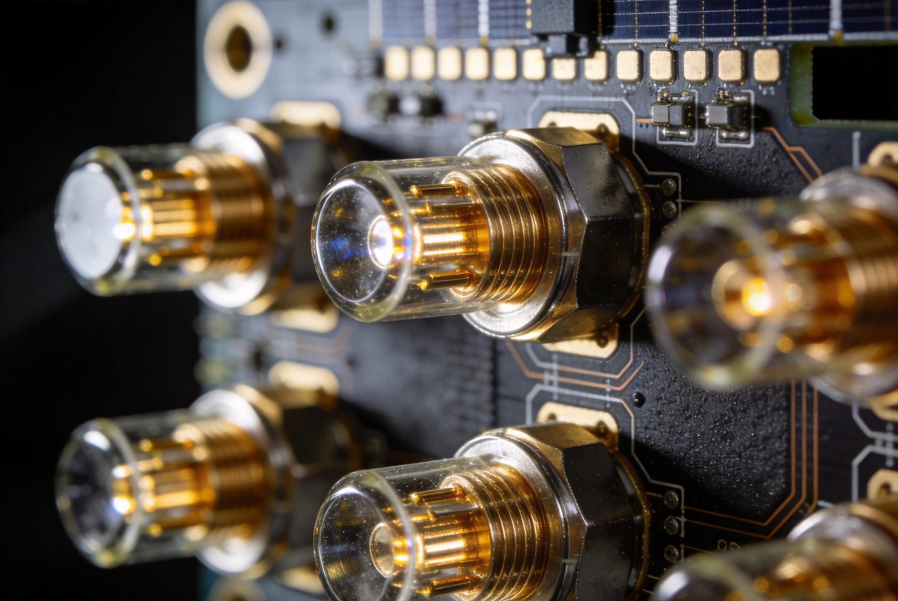
High-Reliability Interconnects for Satellite and Space CommunicationSeptember/18/2026In orbit, 35,786 kilometers above the equator, a communications satellite operates in an environment that is almost perfectly hostile to electronics. It is bombarded by radiation from solar flares and cosmic rays, subjected to extreme thermal cycling as it moves between direct sunlight and the col...
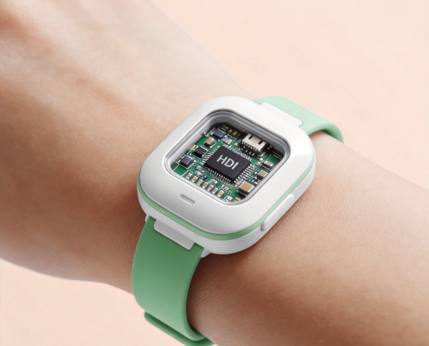
HDI Solutions for Wearable Health Monitors and Diagnostic ToolsSeptember/17/2026The wearable health technology market is experiencing explosive growth, driven by consumer demand for continuous biometric monitoring and clinician demand for ambulatory diagnostic data. From continuous glucose monitors and cardiac event recorders to pulse oximeters and blood pressure watches, the...
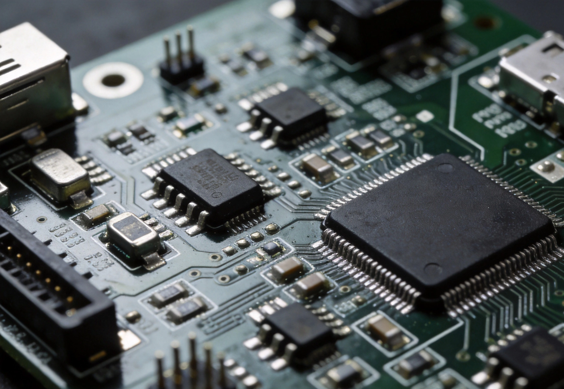
High-Reliability HDI Solutions for PLCs and Motor DrivesSeptember/16/2026Programmable Logic Controllers and motor drives form the operational backbone of modern industrial automation. These systems monitor processes, execute control algorithms, and drive motors with millisecond precision across manufacturing floors that operate around the clock. When a PLC in an automo...
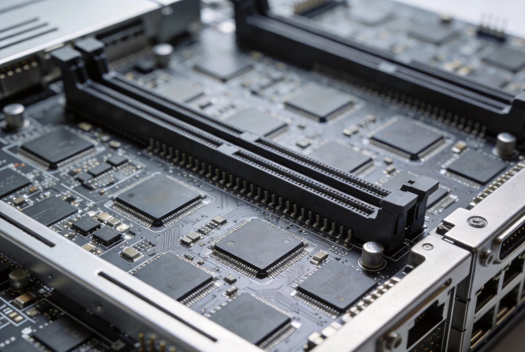
How HDI Technology Supports PCIe Gen5 and Gen6 ComputingSeptember/15/2026The computing industry stands at another bandwidth inflection point. PCIe Gen5 doubled per-lane data rates to 32 GT/s compared to Gen4, and PCIe Gen6 pushes further to 64 GT/s. These increases sound incremental on paper, but the engineering challenges they create are anything but. At 32 GT/s and b...
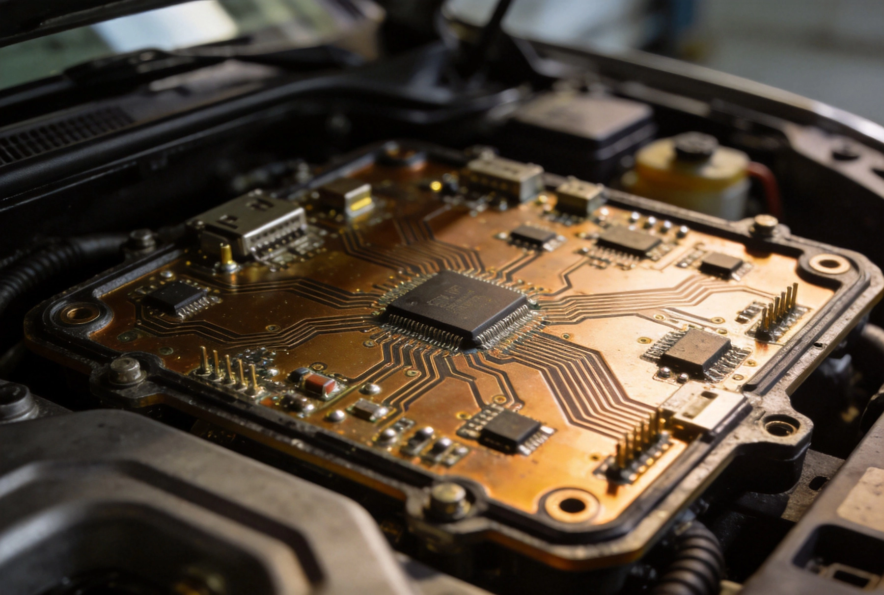
Meeting AEC-Q100 Reliability Standards for Automotive HDISeptember/14/2026Automotive electronics operate in environments that would destroy consumer-grade components. Temperature extremes, vibration, humidity, and the constant demand for zero defects over a 15-year lifespan require a fundamentally different approach to design and manufacturing. For HDI boards destined f...
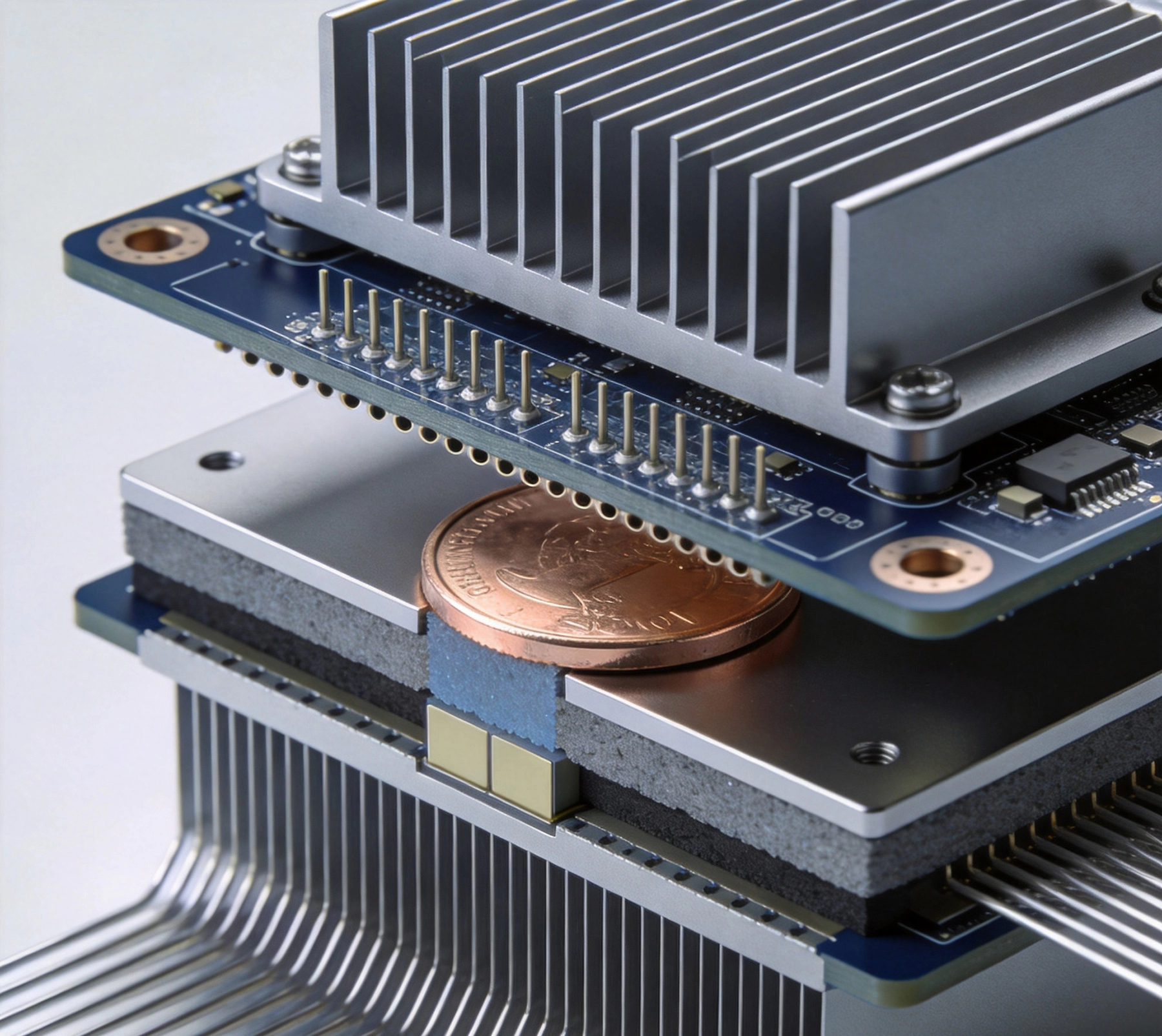
Thermal Management Strategies for HDI Power ModulesSeptember/11/2026Power electronics and high density interconnect (HDI) PCB technologies are increasingly combined in modern electronic systems. Server power supplies, electric vehicle chargers, industrial motor drives, and RF power amplifiers all place demanding thermal requirements on compact HDI boards. The chal...
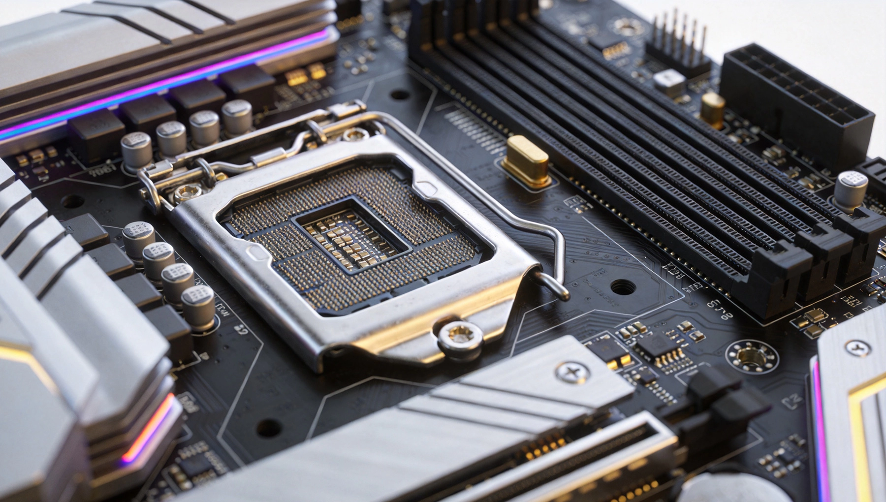
HDI Solutions for High-Performance Gaming Consoles and LaptopsSeptember/10/2026The relentless pursuit of graphical fidelity, processing power, and immersive experiences in modern gaming hardware has pushed printed circuit board technology to its absolute limits. High-performance gaming consoles and laptops demand PCBs that accommodate unprecedented component densities, handl...
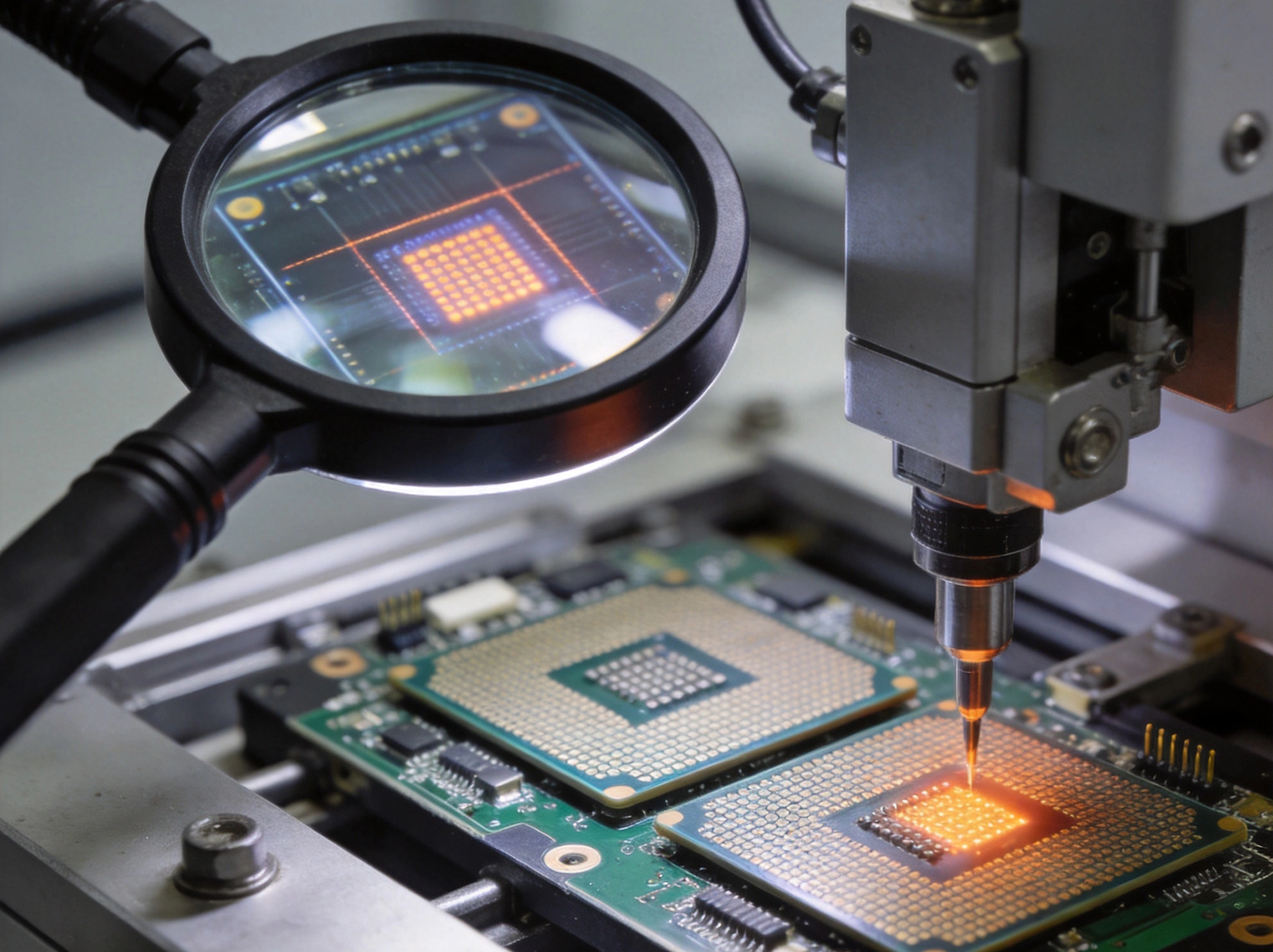
Troubleshooting Common Issues in HDI PCB AssemblySeptember/09/2026High Density Interconnect (HDI) printed circuit boards represent the pinnacle of miniaturization in electronics manufacturing. By utilizing microvias and fine-line geometries, HDI technology enables dramatically increased circuit density while reducing board size and weight. However, these same ch...
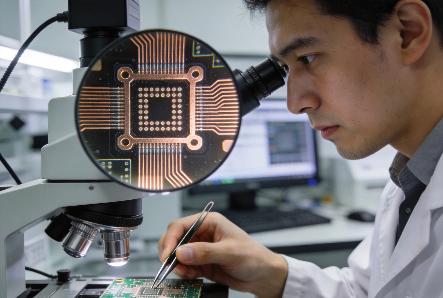
The Role of IPC Standards in HDI PCB Quality AssuranceSeptember/08/2026High Density Interconnect (HDI) PCBs occupy a unique position in the electronics manufacturing landscape: they push the boundaries of what is manufacturable, combining microvia technology, fine-line routing, and advanced materials in structures that are orders of magnitude more complex than the fo...
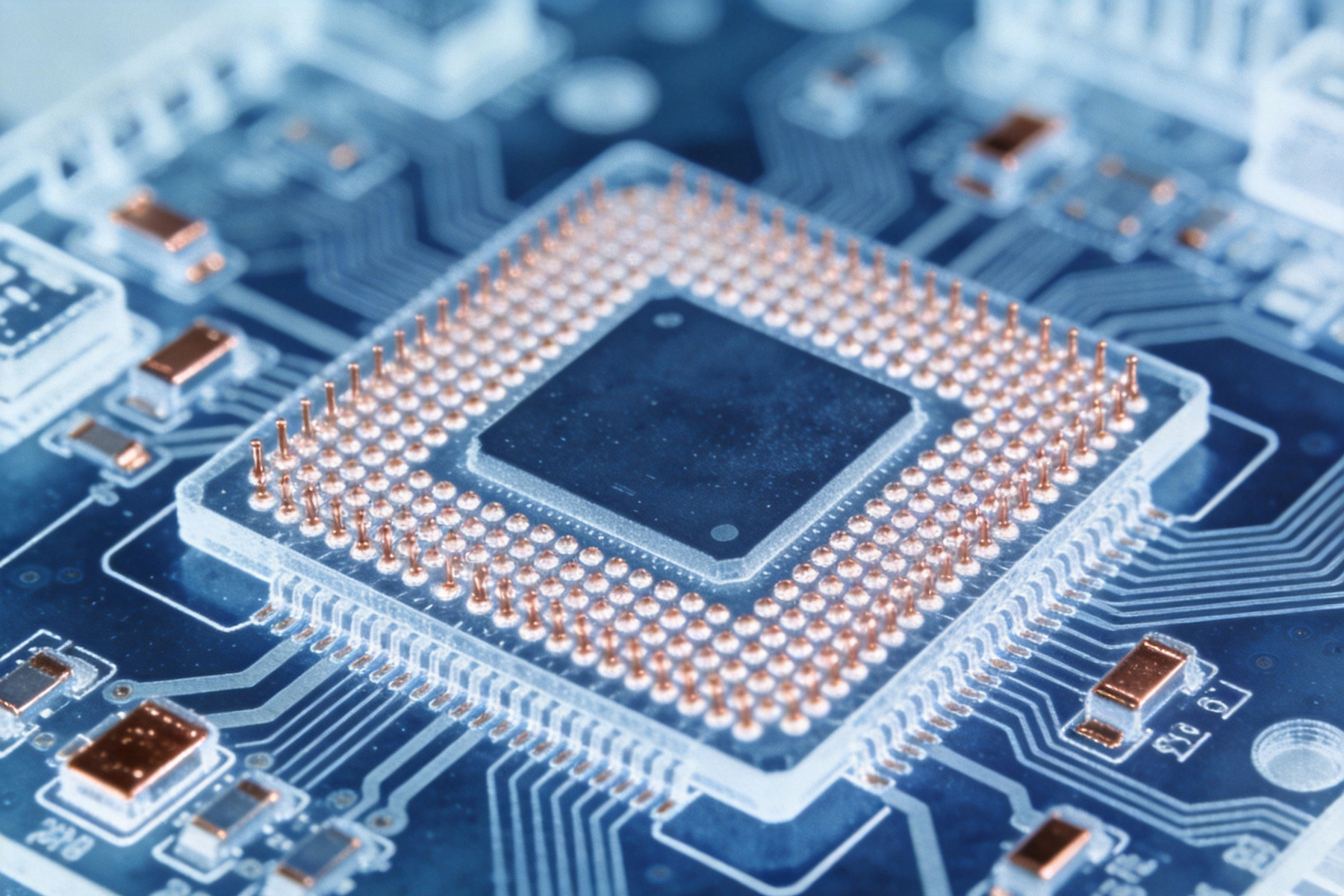
Overcoming the Challenges of Testing Fine-Pitch BGA on HDISeptember/04/2026The semiconductor industry keeps shrinking feature sizes while packing more functionality into each chip. The result: Ball Grid Array packages with pitches of 0.4mm, 0.3mm, and even 0.2mm, mounted on HDI substrates that route signals through microvias and fine traces. This combination delivers rem...
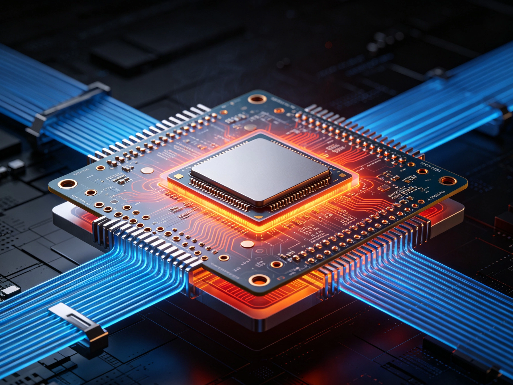
Managing Heat in High-Power HDI Applications: A Practical GuideSeptember/03/2026High-density interconnect (HDI) technology has revolutionized electronics by enabling miniaturization while maintaining or increasing functionality. However, as power densities increase and board real estate shrinks, thermal management becomes one of the most critical challenges facing designers o...