Open Nav

Solar inverters and converters are undergoing a significant transformation. As photovoltaic systems become more powerful, more compact, and more intelligent, the printed circuit boards inside them must handle higher switching frequencies, tighter Thermal Management, and greater functional density. High-density Interconnect, or HDI, technology is increasingly playing a role in meeting these demands.
While Hdi Boards are often associated with smartphones, Wearables, and consumer electronics, their application in solar power equipment is growing. This article explains how Hdi Technology is being used in solar inverters and converters, where it adds value, and what engineering teams should consider when adopting it.
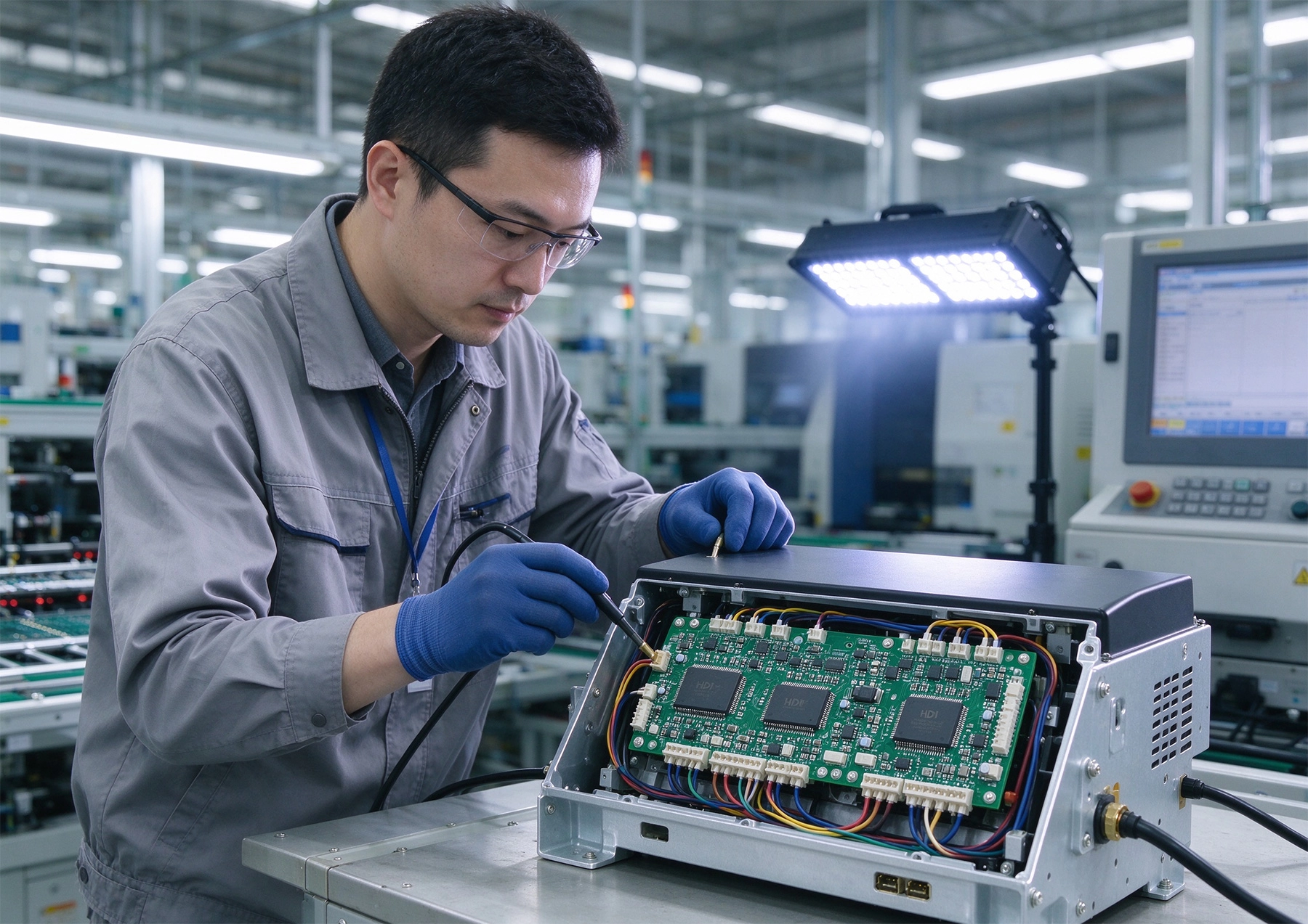
HDI PCBs are printed circuit boards that use finer lines and spaces, smaller vias, higher connection pad density, and more routing layers than conventional boards. Common HDI features include Microvias, Blind Vias, Buried Vias, Via-in-pad structures, and Sequential Lamination processes.
The main advantage of Hdi Technology is that it allows more circuitry to be placed in a smaller area without sacrificing electrical performance. This is achieved by reducing via size, shortening signal paths, and improving layer utilization. For power electronics designers, HDI is not just about Miniaturization. It can also improve switching performance, reduce parasitic inductance, and enable more compact gate driver and control circuits.
Solar inverters convert direct current from photovoltaic arrays into alternating current suitable for grid connection or local consumption. Converters manage voltage levels between different parts of the system, such as DC-DC stages, battery interfaces, and power distribution units. Both functions rely on fast-switching power semiconductors, precise sensing, and robust control electronics.
Several industry trends are increasing PCB complexity in solar power systems:
These trends make conventional PCB layouts less suitable for certain sections of solar power equipment, especially where control, sensing, and gate driving circuits must sit close to high-speed power devices.
Gate driver circuits are critical in solar inverters and converters. They control the switching behavior of power transistors and directly affect efficiency, electromagnetic compatibility, and reliability. With silicon carbide and gallium nitride devices, switching edges become faster, and loop inductance must be minimized.
HDI technology allows shorter gate driver traces, smaller vias, and tighter placement of decoupling capacitors near power devices. This can reduce parasitic inductance, limit voltage overshoot, and improve switching stability. In high-frequency designs, even small reductions in loop area can have a measurable impact on performance.
While power stages handle high voltage and high current, control boards manage measurement, protection, communication, and system coordination. These boards often include microcontrollers, digital signal processors, isolated communication interfaces, current and voltage sensors, and safety circuits.
Hdi Boards are well suited for these sections because they support dense routing, fine-pitch components, and multiple signal layers. This is especially useful in string inverters, hybrid inverters, and modular converter systems where control functionality continues to expand.
Residential solar inverters are under strong pressure to become smaller, lighter, and easier to install. Wall-mounted and compact outdoor units leave limited space for PCBs, connectors, cooling structures, and safety clearances.
By using HDI technology in control and auxiliary sections, manufacturers can reduce board size, consolidate functions, and maintain adequate creepage and clearance distances on power sections. This helps achieve higher power density without overcomplicating mechanical design.
Hybrid inverters and battery converters add another layer of complexity. They must manage bidirectional power flow, Battery Management System communication, DC coupling, and grid interaction. These systems often require more sensing channels, isolation barriers, and communication interfaces than traditional string inverters.
HDI boards can help integrate these functions into fewer layers or smaller footprints, particularly in digital control modules, isolated communication sections, and sensor interface circuits.
Solar inverters and converters operate at high voltages, sometimes exceeding 1,000 V DC in utility-scale systems. Safety standards require sufficient creepage and clearance distances to prevent arcing and ensure long-term insulation reliability.
HDI technology does not replace these requirements. Instead, it is typically applied to low-voltage control sections, gate drivers, communication circuits, and sensor interfaces. High-voltage power paths still need careful spacing, slotting, conformal coating, and insulation design.
HDI boards use thinner dielectric layers and smaller vias, which can affect thermal behavior. In solar power equipment, heat is generated by power semiconductors, magnetics, and resistive losses. If HDI sections are placed near hot components, Thermal Vias, copper pours, and substrate selection must be evaluated carefully.
For high-power areas, metal-core PCBs, thick copper layers, or ceramic substrates may still be more appropriate. HDI is most effective when used where signal density and switching performance matter more than bulk current carrying capacity.
Solar inverters often operate in demanding environments, including rooftop installations, outdoor cabinets, and industrial facilities. Pcb Materials must withstand temperature cycling, humidity, and long-term electrical stress.
High-reliability HDI boards for solar applications may require high-Tg laminates, Low-loss Materials for high-frequency signals, and robust via structures. Material choices should be validated against the expected operating temperature, humidity class, and product lifetime.
Fast-switching power devices generate high-frequency noise that can interfere with control circuits, sensors, and communication interfaces. HDI layouts can help by shortening critical loops and improving grounding, but they also require careful stack-up planning.
Designers should pay attention to return current paths, shielding layers, separation between noisy and sensitive circuits, and via placement around high-speed nodes. A dense layout without proper EMC planning can make compliance testing more difficult.
HDI PCBs are more complex to manufacture than conventional boards. Processes such as Laser Drilling, Sequential Lamination, Via Filling, and fine-line imaging increase production cost and lead time. Not all PCB suppliers have mature HDI capability for high-reliability industrial applications.
For solar equipment, the key is to apply HDI selectively. Using HDI only where it delivers clear electrical or mechanical benefits can control cost while still improving overall system performance.
Solar inverters and converters are expected to operate for 10 to 25 years, depending on the application. This long service life places strict demands on Pcb Reliability. HDI structures must survive thermal cycling, vibration, humidity, and repeated power transients.
Via reliability is particularly important. Microvias, Blind Vias, and Via-in-pad structures must be designed and manufactured to avoid early failures. Plating quality, via aspect ratio, resin filling, and solder mask coverage should be reviewed during the design-for-manufacturability stage.
Qualification testing may include thermal cycling, power cycling, humidity bias testing, insulation resistance measurement, and mechanical stress evaluation. These tests help confirm that HDI features will remain reliable over the product lifetime.
HDI technology is powerful, but it is not necessary for every solar Pcb Design. Conventional multilayer boards may still be more suitable when:
The best approach is often a hybrid strategy. High-density HDI boards can be used for control, sensing, and gate driver sections, while conventional or specialized boards handle high-voltage and high-current power stages.
HDI technology is becoming increasingly relevant in solar inverters and converters, especially as power electronics move toward higher switching frequencies, smaller enclosures, and more integrated functionality. It offers clear benefits for gate driver layout, control board density, electromagnetic performance, and system Miniaturization.
However, HDI adoption in solar power equipment must be balanced against safety, thermal, reliability, and cost considerations. It is not a universal replacement for conventional Pcb Technology, but a targeted tool that can improve performance where density and high-speed behavior matter most. When applied thoughtfully, HDI can help solar inverter and converter manufacturers build more compact, efficient, and reliable power systems.
HDI is not yet universal in solar inverters, but its use is growing in control boards, gate driver circuits, communication modules, and compact residential inverters. High-voltage power stages often still use conventional or specialized PCB technologies.
HDI itself does not directly increase conversion efficiency, but it can enable better layout for high-speed switching devices. Shorter loops, reduced parasitic inductance, and improved gate driver placement can help reduce switching losses and electromagnetic interference.
Yes, when properly designed and manufactured. HDI boards used in solar applications should be qualified for thermal cycling, humidity, and long-term electrical stress. Supplier capability, via design, material selection, and inspection processes are critical to reliability.
HDI boards typically cost more than conventional multilayer boards due to additional manufacturing steps. However, the total system cost may still improve if HDI enables smaller enclosures, fewer layers, better performance, or simplified assembly.
The Role of HDI PCBs in Miniaturized Implantable Medical DevicesJuly/21/2026
Why IoT Sensors Rely on High-Density Interconnect TechnologyOctober/13/2026
High-Reliability Standards for HDI in Life-Critical Healthcare EquipmentAugust/11/2026
HDI Solutions for Wearable Health Monitors and Diagnostic ToolsSeptember/17/2026
The Role of HDI Technology in Wearable Device MiniaturizationJuly/15/2026
Exploring the 6 Types of HDI Structures: From Type I to Any-LayerAugust/14/2026
The Role of HDI in Robotics and Motion Control SystemsAugust/10/2026
The Impact of Via-in-Pad on Thermal Performance and ReliabilitySeptember/26/2026