
Every time someone straps on a smartwatch or pops in wireless earbuds, they're carrying miniature engineering marvels. These devices pack processing power that would have required a desktop computer a decade ago into form factors smaller than a matchbox. At the heart of this shrinking revolution sits a technology that most consumers never see: HDI printed circuit boards.
HDI—High Density Interconnect—technology isn't new. Military and aerospace applications have used it for decades. But the demands of consumer Wearables have pushed HDI into the mainstream, driving innovation in manufacturing processes and design techniques that benefit the entire electronics industry.
Understanding HDI's role in wearable Miniaturization helps engineers, product managers, and procurement professionals make better design decisions and communicate more effectively with manufacturing partners.
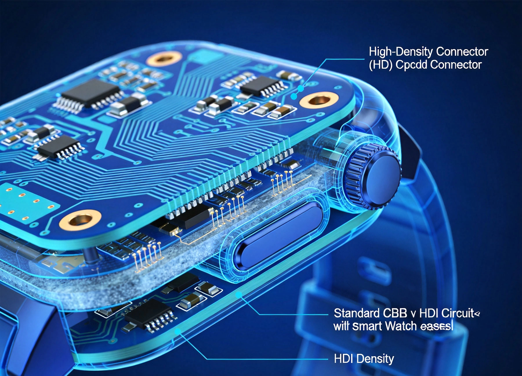
Standard PCBs connect layers through mechanical drill holes—plated through holes (PTH) that must be large enough for reliable plating. These holes consume significant board space and limit routing density. HDI flips this approach, using laser-drilled Microvias that are dramatically smaller and can be placed anywhere on the board surface.
The difference is fundamental: where standard vias might measure 0.3mm to 0.5mm diameter, HDI Microvias range from 0.1mm down to 0.05mm or smaller. This isn't incremental improvement—it's an order-of-magnitude reduction in via footprint that cascades into routing density improvements throughout the board.
Three technical characteristics define Hdi Boards:
Microvias: Laser-drilled holes connecting adjacent layers, typically 0.1mm diameter or smaller. These vias have much lower aspect ratios than mechanical holes, making them more reliable and allowing finer line geometries.
Fine line widths and spacing: HDI processes achieve trace widths of 75μm (3 mil) or less compared to 100μm to 150μm for standard boards. Tighter spacing enables more routing in less area.
Any-layer interconnect: Advanced HDI allows vias connecting any two layers—not just sequential buildup—which maximizes routing flexibility and reduces layer count requirements.
Consumer Wearables create Pcb Design challenges that standard boards struggle to address.
A smartwatch motherboard might measure 20mm × 30mm. An earbud processing board perhaps 10mm × 20mm. These tiny areas must accommodate processors, wireless chips, power management, sensors, and all the routing between them.
Standard Pcb Design with 0.15mm traces and 0.3mm vias simply cannot fit in these spaces. HDI's finer features pack 2x to 3x more routing into equivalent area, enabling complex functionality in cramped form factors.
Wearable processors are increasingly complex: Bluetooth/WiFi combos, application processors, power management ICs, audio codecs, and sensor interfaces—all in packages smaller than your fingernail. These components need high pin counts with fine pitch—0.4mm BGA spacing is common, 0.3mm appears increasingly.
Standard boards struggle to fan out these fine-pitch packages. HDI's microvias can be placed directly beneath component pads (Via-in-pad), eliminating fan-out routing entirely and reducing the area needed for high-density components.
Wearable devices increasingly combine functions that previously required separate boards: application processing, wireless connectivity, sensor management, power delivery, and audio. Integrating these functions on fewer boards saves space and reduces assembly complexity.
HDI enables this integration through blind and Buried Via structures that connect internal layers without consuming surface routing area. A 6-layer HDI board can provide routing density equivalent to 10 or 12 layers on standard technology.
Different HDI construction approaches offer tradeoffs suited to specific wearable applications.
SBU builds Hdi Boards layer by layer, drilling microvias after each dielectric layer application. This method offers maximum design flexibility but requires more manufacturing steps. For complex wearable boards with many internal connections, SBU provides the routing access needed.
The process involves alternating dielectric coating, Microvia formation, and Copper Plating. Each cycle adds cost but enables increasingly complex layer stacking. Most HDI wearables use 3 to 6 buildup cycles maximum to control cost.
mSAP starts with very thin copper on dielectric and adds copper in precise patterns, enabling finer line geometries than standard processes. This approach achieves 30μm to 50μm trace widths—essential for the highest-density wearable applications.
Smartphone motherboards pioneered mSAP technology, and the techniques have transferred to wearables where similar density requirements exist. The process requires precise process control but delivers exceptional routing density.
Some HDI constructions embed passive components—resistors and capacitors—within the board layers rather than mounting them on the surface. This recovers surface area for other components or reduces board size for equivalent functionality.
Embedded passives work well for high-volume applications where design costs amortize over millions of units. For wearables with moderate volumes, surface-mount passives typically remain more cost-effective despite consuming board space.
HDI offers several via types, each suited to specific applications.
The simplest HDI via connects two adjacent layers. TMVs are the fastest to manufacture and most reliable for high-density applications. Since they don't penetrate deep into the board stack, thermal stress affects them less than through-hole vias.
For wearable designs, TMVs connecting layer 1 to layer 2 serve most via requirements. This simplicity improves manufacturing yield and reduces cost compared to more complex via structures.
Blind Vias connect an outer layer to one or more inner layers without penetrating through the entire board. They enable routing from surface components to internal layers without consuming space for through-hole transitions.
In wearables, blind microvias from the top layer to internal ground and power planes reduce the via stub effects that degrade signal quality at high frequencies.
Microvias can be staggered (offset between layers) or stacked (directly over each other between multiple layer pairs). Stacked vias enable higher routing density but require more precise manufacturing to ensure reliable connection between layers.
For most wearable applications, staggered microvias provide adequate density with better manufacturing margin. Reserve stacked vias for the highest-density areas where every micrometer matters.
Effective HDI Stack-up Design balances electrical performance, manufacturing capability, and cost constraints.
The most aggressive Miniaturization uses HDI to reduce total layer count compared to standard designs. A 4-layer HDI board might replace a 6-layer standard design, reducing thickness and weight while improving routing density.
However, fewer layers require more careful planning to manage Impedance Control, signal isolation, and power distribution. Electrical simulation helps validate stack-up choices before committing to manufacturing.
Typical wearable HDI stack-ups range from 4 to 8 layers:
Beyond 8 layers, manufacturing cost and complexity escalate significantly. Most consumer wearables stay at 6 layers or fewer.
Wearable device thickness constraints—typically 5mm to 10mm total—limit PCB thickness to 0.4mm to 0.8mm. HDI enables this reduction because microvias require less total thickness than equivalent through-hole constructions.
Work closely with your manufacturer on thickness targets. Their layer thickness capabilities, Dielectric Material choices, and lamination processes all affect achievable board thickness.
Material selection affects HDI performance, manufacturability, and cost.
Standard FR-4 works for some Hdi Applications but limited thermal and electrical performance. High-Tg materials—TMA150 or higher—better resist the thermal cycling wearables experience during use and charging.
For advanced applications with high-frequency wireless signals, low-Dk materials (Df below 0.01 at GHz frequencies) reduce signal losses. These materials cost more but enable better wireless performance in space-constrained designs.
Sequential buildup uses either buildup film (ABF) or prepreg as dielectric layers. ABF provides excellent thickness control and planar surfaces ideal for fine-pitch components but costs more. Prepreg is less expensive but may require more process control for consistent results.
For most wearable applications, ABF or equivalent buildup film delivers the surface quality that dense component packages require.
Standard 1oz copper may be too thick for fine HDI traces. Many manufacturers recommend 0.5oz or even 0.33oz copper for the finest features. However, thin copper limits current capacity in power distribution layers.
Balance copper weight across layers: heavier copper for power/ground planes, thinner copper for fine signal routing. Your manufacturer can recommend appropriate configurations for your specific design.
HDI design rules differ from standard PCB design. Following manufacturability guidelines improves yield and reduces cost.
Microvia diameter is typically 0.1mm to 0.15mm. The capture pad—the copper land where the microvia lands on a layer—should be 0.25mm minimum diameter to ensure reliable registration. Annular Ring around the via should be at least 50μm.
Via pitch—center-to-center spacing between adjacent microvias—should be at least 0.35mm to 0.4mm for standard HDI processes. Tighter pitch is possible but increases cost and reduces manufacturing margin.
Achievable trace widths depend on copper weight and manufacturing process:
Match your design rules to your manufacturer's actual capabilities. Aggressive design rules beyond manufacturer capability produce manufacturing failures.
Microvia formation and plating require clearances around component pads and other features. Discuss your manufacturer's specific keep-out requirements during design—these vary between shops and processes.
Typical requirements: 0.15mm clearance from microvia capture pads to adjacent routing, 0.2mm clearance around blind microvia locations for processing tolerances.
Compact HDI assemblies generate concentrated heat that must dissipate through limited thermal paths.
Thermal Vias connect components to internal ground planes that spread heat. For high-power components, thermal via arrays beneath the package—often 3×3 to 5×5 patterns—provide critical Heat Dissipation paths.
Via fill or plug processes ensure void-free Copper Plating in thermal via arrays. Empty Thermal Vias trap air, which insulates rather than conducts heat.
For the most demanding thermal applications, metal-core substrates—aluminum or copper cores with dielectric and copper layers—provide superior Thermal Conductivity. These boards cost significantly more but handle power densities impossible with standard dielectrics.
Metal-core boards also enable integrated heat spreading, potentially eliminating separate heat sink components. This trades board cost against device-level simplification.
Given the complexity of thermal paths in HDI assemblies, Thermal Simulation has moved from optional to essential. CFD (Computational Fluid Dynamics) and FEA (Finite Element Analysis) tools predict thermal behavior and identify hotspots before physical prototypes.
Many HDI manufacturers provide Thermal Simulation services or can recommend specialized design consultants. Budget for this analysis in your development schedule.
HDI costs more than standard Pcb Technology, but the premium often makes sense when total system cost is considered.
Hdi Manufacturing involves more steps than standard PCB production:
Compared to standard 6-layer boards, equivalent HDI boards typically cost 50% to 100% more. For high-volume products, this premium may be acceptable; for lower volumes, the per-board cost can be challenging.
Several strategies reduce HDI cost premium:
HDI cost follows classic economies-of-scale curves. At 1,000 units, per-board costs reflect significant setup amortization. At 100,000 units, setup costs spread across many boards and material purchasing power dominates. Understand where your volume sits on this curve when budgeting.
Not all PCB manufacturers handle HDI equally well. Selection matters significantly.
Ask potential manufacturers for:
Request sample boards or customer references for similar complexity levels.
Quality HDI manufacturers offer design review services that catch manufacturability issues before production. Take advantage of this—catching a design rule violation before tooling costs nothing; catching it after causes expensive respins.
Provide complete design files, stack-up specifications, and intended use conditions. The more context your manufacturer has, the better their review.
HDI boards require more detailed documentation than standard PCBs:
Prepare documentation early in discussions with manufacturers to avoid misunderstandings.
Hdi Technology continues evolving to meet ever-more-demanding wearable requirements.
Research continues on even finer features: sub-50μm traces, sub-0.1mm microvias, and embedded active components. While not yet mainstream, these technologies will appear in future wearables as manufacturing processes mature.
Fan-out wafer-level packaging (FOWLP) and similar approaches blur the line between IC packaging and PCB, potentially eliminating Traditional Pcb approaches entirely for some applications.
Additive manufacturing for electronics—3D-printed circuits—remains experimental but offers intriguing possibilities. True 3D circuit structures could revolutionize wearable form factors by embedding wiring within mechanical structures rather than planar boards.
Current limitations in material conductivity and manufacturing throughput keep this technology away from production applications, but monitoring its development makes sense for forward-looking product planners.
Hdi Technology is essential to wearable device miniaturization—not optional, but foundational. The routing density, via flexibility, and layer efficiency HDI provides enable the functionality consumers expect from devices they can comfortably wear.
Understanding HDI characteristics—microvia construction, layer stacking, design rules, and material considerations—helps product teams make better tradeoffs and communicate more effectively with manufacturing partners.
The cost premium for HDI often pays for itself through system-level savings: fewer boards, simpler assemblies, smaller enclosures, reduced weight. When evaluating total wearable product cost, HDI's contribution becomes clear.
As wearables continue adding capabilities while shrinking form factors, HDI technology advances in parallel. The boundary between possible and impossible in wearable design keeps shifting outward—HDI technology is why.
Production microvia diameters of 0.1mm are standard across most HDI manufacturers. Advanced processes achieve 0.075mm, and some research processes have demonstrated 0.05mm vias. Match your via requirements to your manufacturer's actual production capabilities.
HDI and flex circuits serve different needs. HDI provides maximum routing density in rigid form factors; flex provides mechanical flexibility and 3D packaging options. Many advanced wearables use both—HDI rigid boards for processing functions, flex or rigid-flex for connections and mechanical integration.
Properly designed and manufactured HDI meets or exceeds standard Pcb Reliability. Microvia Reliability actually benefits from lower thermal expansion mismatch due to shorter span. The key is working within manufacturer-qualified design rules and stack-ups rather than pushing beyond proven capabilities.
HDI repair is significantly more difficult than standard PCB repair. Microvia access is limited, and layered construction complicates rework. This makes first-pass quality—through design optimization and process control—more critical than for standard boards.
HDI can improve Signal Integrity through shorter via stubs, better controlled impedance due to thinner dielectrics, and more routing flexibility. However, fine traces require more careful impedance control and may be more susceptible to manufacturing variation.
Consumer electronics demand—especially smartphones—has driven massive investment in Hdi Manufacturing capability and yield improvement. Techniques developed for high-volume smartphone production now benefit lower-volume wearable applications through shared manufacturing learning.
This article is intended for informational purposes. Consult with qualified PCB design engineers and HDI manufacturing partners for specific application guidance.
Using HDI Technology in Solar Inverters and ConvertersOctober/14/2026
High-Reliability Standards for HDI in Life-Critical Healthcare EquipmentAugust/11/2026
Why IoT Sensors Rely on High-Density Interconnect TechnologyOctober/13/2026
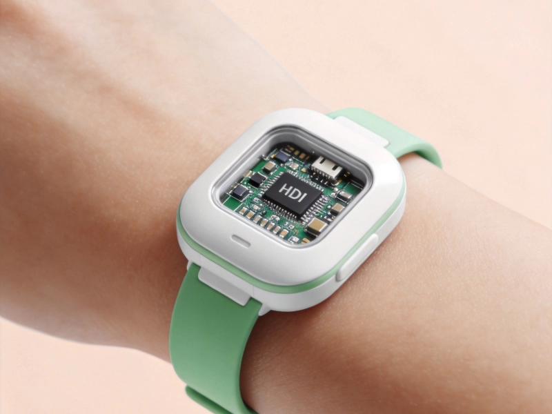
HDI Solutions for Wearable Health Monitors and Diagnostic ToolsSeptember/17/2026
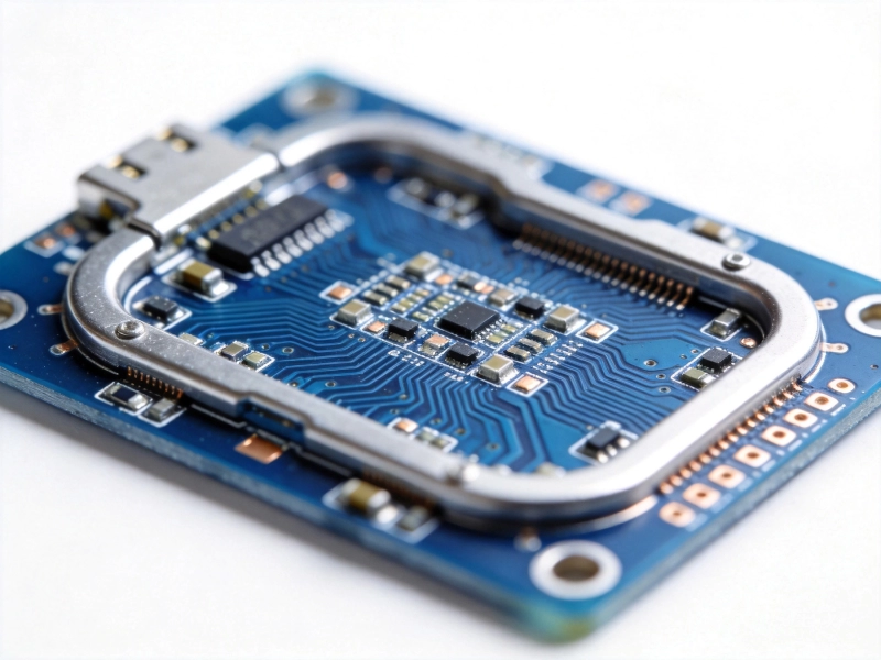
The Role of HDI PCBs in Miniaturized Implantable Medical DevicesJuly/21/2026
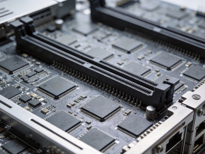
How HDI Technology Supports PCIe Gen5 and Gen6 ComputingSeptember/15/2026
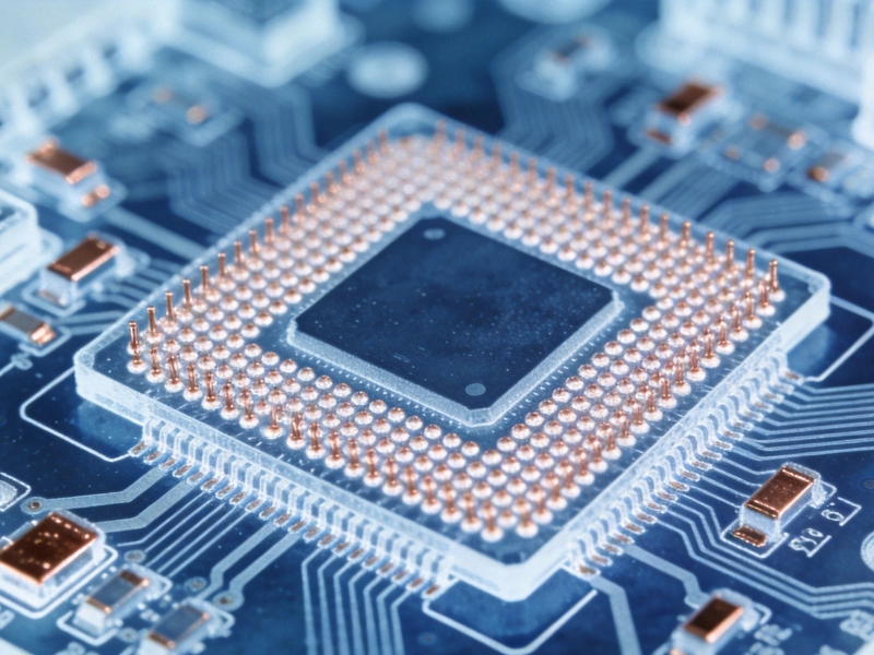
Overcoming the Challenges of Testing Fine-Pitch BGA on HDISeptember/04/2026

HDI Solutions for In-Vehicle Infotainment (IVI) and ClustersAugust/07/2026