Open Nav

Testing High-density Interconnect (HDI) PCBs presents unique challenges that traditional Pcb Testing Methods simply cannot address. The microscopic features, Buried Vias, and ultra-fine pitch components that make Hdi Technology powerful also make them extraordinarily difficult to inspect and test. A single missed defect in an HDI assembly — whether it's a Microvia void, an insufficient solder joint, or a buried trace flaw — can cause field failures that damage reputations and increase warranty costs. This guide explores every major advanced testing method for HDI PCBs, from Automated Optical Inspection to 3D X-ray computed tomography, so you can understand how quality is ensured in the world's most sophisticated electronic assemblies.
Conventional PCBs with through-hole technology and surface mount components with 0.5mm+ pitch are relatively straightforward to test. Human inspectors can visually verify solder joints, and standard test equipment can probe accessible nodes. HDI PCBs break these assumptions in multiple ways that demand fundamentally different testing approaches.
The HDI Microvia — the defining feature of Hdi Technology — creates test access challenges that conventional flying probe or bed-of-nails testers cannot overcome. With via diameters of 0.1mm to 0.3mm and pad diameters often under 0.4mm, there's simply no physical probe that can reliably contact these structures without risking damage. Even where probe access exists, the number of test points may be thousands per square centimeter, making traditional node-by-node testing impossibly slow.
Layer counts in advanced Hdi Boards can reach 12, 16, or even 20+ layers, with many layers containing only power and ground planes — no accessible circuitry for probing. Defects in these buried layers are invisible to any external inspection method and can only be detected through specialized techniques like thermal cycling stress testing or cross-sectional analysis. The consequences of missing such defects include field failures that appear as intermittent operation, complete board failure, or — in safety-critical applications like automotive or medical — potentially hazardous situations.
No single Hdi Pcb testing method can detect all possible defects. A robust quality strategy combines multiple complementary techniques, each addressing specific defect categories. The testing pyramid below illustrates this layered approach:
Foundation layer: test points, JTAG boundaries, design rules that enable effective testing
AOI, 3D SPI, and manual inspection for solder joint quality and component placement
ICT, flying probe, Boundary Scan for opens, shorts, and component values
2D/3D X-ray, SAT for hidden solder joints, microvia integrity, delamination
In-system programming, functional test, burn-in for system-level verification
Thermal cycling, shock, vibration, humidity for long-term durability
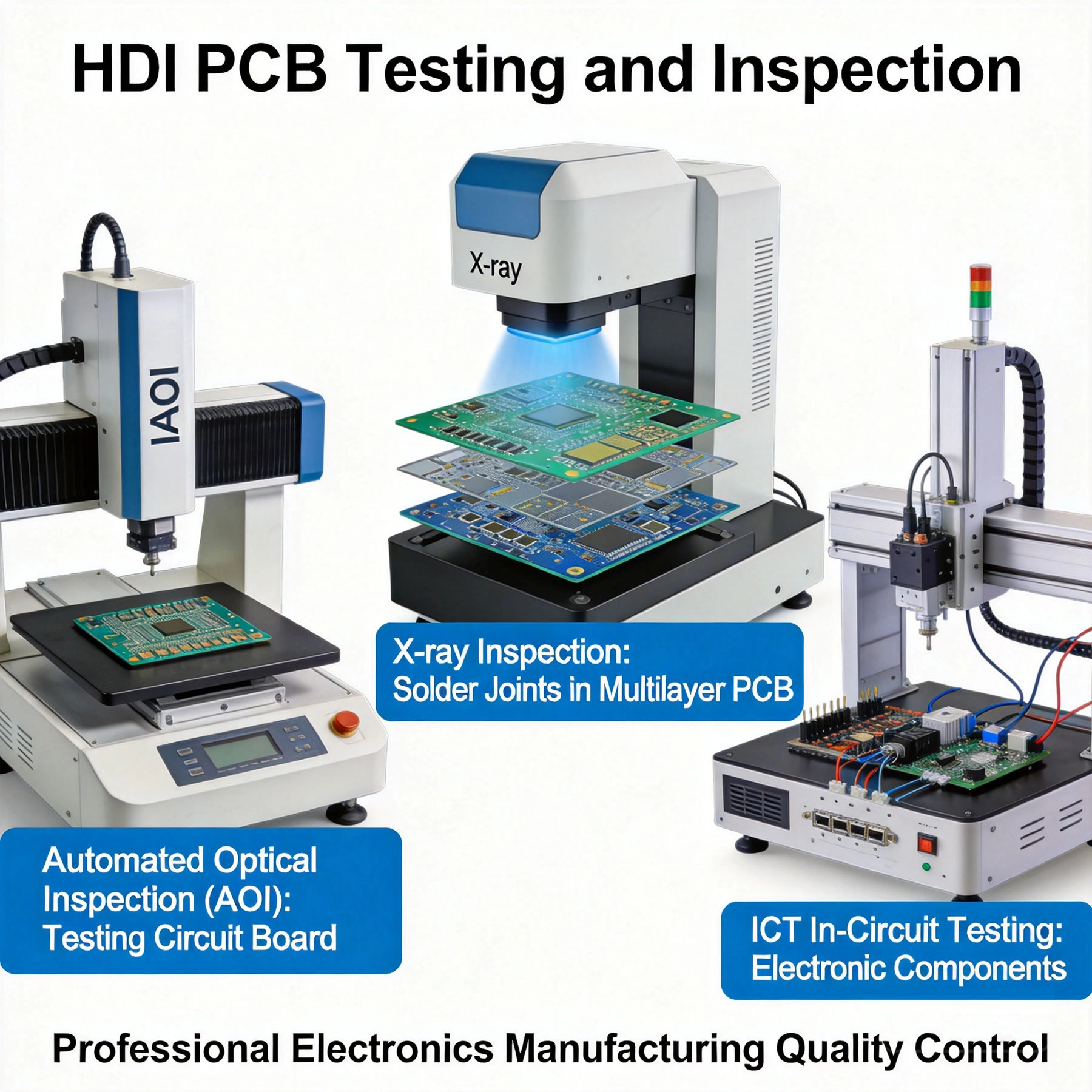
Automated Optical Inspection (AOI) uses high-resolution cameras and sophisticated image processing algorithms to inspect PCB assemblies for defects. Modern AOI systems can detect component presence/absence, polarity errors, tombstoning, offset placement, insufficient or excess solder, bridging, and damaged components. For HDI assemblies, AOI is typically deployed after solder paste inspection (SPI) and again after reflow.
AOI systems use multiple camera angles — typically top-down and oblique (side-view) — to capture images of the entire assembly. For HDI PCBs with ultra-fine pitch components (0.3mm and 0.4mm pitch BGAs, QFNs, and chip-scale packages), resolution requirements exceed 10 megapixels with pixel sizes below 10 microns. Some advanced AOI systems use structured light projection for 3D measurement, enabling accurate solder volume assessment even on uneven surfaces.
AOI cannot inspect hidden solder joints — the area under BGAs and QFNs where the most critical connections are made. This blind spot requires complementary inspection methods. Additionally, AOI systems can generate false calls (flagging good joints as defective) or miss defects that don't produce visible signatures, particularly in cases of hidden voids or micro-cracks. Typical AOI defect escape rates of 5-15% for complex assemblies mean that AOI alone is insufficient for high-reliability HDI products.
Solder Paste Inspection (SPI) is performed after paste printing but before component placement. By catching solder volume errors early, SPI prevents defects rather than detecting them after reflow, when rework becomes necessary. For HDI assemblies with fine-pitch components, SPI is particularly critical — a solder bridge caused by excess paste or a cold joint caused by insufficient paste is nearly impossible to rework on 0.3mm pitch components without damaging adjacent features.
HDI assemblies with ultra-fine pitch components require tight SPI tolerances. For a 0.4mm pitch BGA with 0.2mm pads, the acceptable solder volume tolerance may be ±10% or tighter. 3D SPI systems with resolution below 5 microns can meet these requirements, while older 2D systems may lack the precision needed for today's densest HDI assemblies. When specifying SPI requirements for HDI work, verify that your contract manufacturer's equipment can meet the tolerances your components require.
X-ray Inspection is the essential complement to AOI for HDI assemblies — the only practical method for examining hidden solder joints and internal PCB structures. X-rays pass through most materials (except metals and high-density ceramics), creating images that reveal internal features invisible to optical inspection. For HDI PCBs with buried components and BGA packages, X-ray is not optional — it's mandatory for quality assurance.
Standard 2D X-ray systems project X-rays through the assembly onto a detector, creating a 2D image similar to medical radiography. Metal structures (solder joints, component leads, copper traces) appear bright; organic materials (PCB substrate, components) appear dark. 2D X-ray is effective for:
X-ray CT scanning takes multiple 2D X-ray images as the assembly rotates, then reconstructs a complete 3D volume model of the board. This enables:
For production-speed inspection of hidden joints, some manufacturers use 2.5D X-ray systems (also called laminography or tomosynthesis) that acquire multiple images and computationally reconstruct specific planes while blurring others. This provides intermediate capability between 2D X-ray and full CT — faster than CT but more informative than 2D. Laminography is commonly used for Bga Inspection on production lines where 100% inspection is required.
In-Circuit Testing (ICT), also called bed-of-nails testing, uses a fixture with spring-loaded probes that contact specific test points on the PCB. ICT verifies correct component values (resistance, capacitance, inductance), checks for opens and shorts in the circuit, and validates that each component is properly connected in the circuit. For HDI assemblies, ICT is complicated by the reduced accessibility of test points, but remains valuable for boards where adequate test access was designed in.
The primary challenge for ICT on HDI assemblies is test point accessibility. With components placed on both sides, ultra-fine pitch connections, and buried vias, there may simply be no physical location to probe many circuit nodes. Standard grid arrays of probes require minimum 2mm pitch, which is incompatible with the feature densities of advanced HDI. These limitations mean:
When Hdi Boards must be ICT-tested, design for testability (DFT) becomes critical. This means:
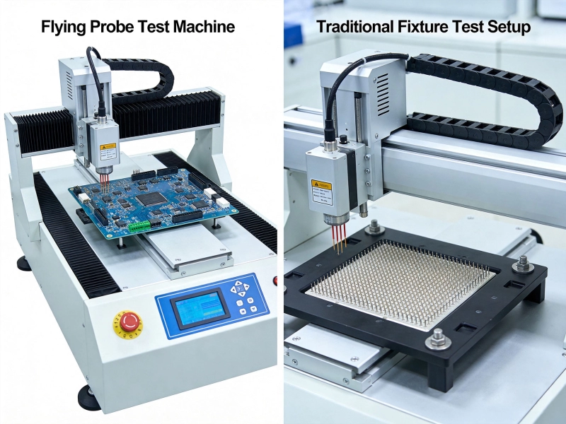
Flying probe testing addresses the fixture cost and accessibility challenges of ICT by using movable probes that travel to each test point rather than a fixed bed-of-nails fixture. Flying probe systems have two to six probe heads that move independently, making contact with test points as needed for each measurement. For prototype and low-to-medium volume HDI production, flying probe offers significant advantages over traditional ICT.
The tradeoff for flying probe's flexibility is speed. With sequential probing (probes move to each test point one at a time), test time scales with the number of test points. A comprehensive Flying Probe Test on a complex HDI board might take 10-30 minutes, compared to seconds for ICT. This makes flying probe unsuitable for high-volume production where cycle time is critical. Flying probe is the right choice for:
Boundary scan, defined by the IEEE 1149.x family of standards (commonly called JTAG after the Joint Test Action Group that originated the technology), is a method for testing interconnections between integrated circuits without requiring physical probe access to each node. By embedding scan cells within each IC, boundary scan enables test pattern insertion and response capture through a standard 4-wire or 5-wire interface, regardless of the IC package density.
Boundary scan cells are placed at each IC pin (input, output, and bidirectional). During test mode, these cells form a long shift register — the boundary scan chain — that can shift in test data and shift out responses. This enables:
Boundary scan is particularly valuable for Hdi Pcb testing because it bypasses the physical accessibility limitations of traditional test methods. With properly designed-in boundary scan:
The original IEEE 1149.1 standard handles DC-coupled interconnections (CMOS and TTL logic). IEEE 1149.6 extends boundary scan to AC-coupled interconnections (high-speed differential signals like Ethernet, USB, HDMI, PCIe). For modern HDI assemblies with high-speed interfaces, 1149.6 boundary scan provides additional coverage that 1149.1 alone cannot achieve.
Scanning Acoustic Microscopy (SAM), also called ultrasonic inspection or acoustic C-scan, uses high-frequency ultrasound to inspect internal PCB structures. Unlike X-rays, acoustic waves are sensitive to material boundaries — they reflect off interfaces between different materials (copper-to-substrate, substrate-to-air, solder-to-component). This makes SAM particularly sensitive to delamination, voids, and moisture absorption that X-ray may miss.
SAM requires a coupling medium (typically deionized water) between the transducer and the board, which limits inspection to offline or batch-mode operation — not inline production testing. Additionally, metal layers reflect ultrasound, creating acoustic "shadows" that limit inspection to specific layers at a time. Despite these limitations, SAM is an essential tool for Hdi Reliability qualification and failure analysis.
Functional testing verifies that the assembled PCB performs its intended functions, rather than testing individual components or connections. Functional test applies power, inputs, and stimulus signals to the board and verifies correct outputs and behavior. For complex HDI assemblies like smartphone main boards or network switch cards, functional test may include:
Burn-in testing operates the board at elevated temperature (typically 70-85°C) with power applied for an extended period (24-168 hours) to accelerate infant mortality failures. Boards that pass burn-in have demonstrated basic functionality under stress and are less likely to fail in the field within the early failure period. For automotive, medical, and industrial applications, burn-in is often a quality requirement specified by the end customer.
Functional test catches board-level issues but is not a substitute for individual defect detection. A board with 5% marginal solder joints might pass functional test if the marginal joints happen to make adequate contact during the test period, then fail in the field when thermal cycling or vibration causes further degradation. Functional test is most effective when combined with the defect-detection methods described earlier — AOI, X-ray, and electrical testing catch the defects that functional test might miss.
For HDI PCBs used in demanding environments, reliability testing verifies that the assembly will perform throughout its intended service life. These tests simulate years of operational stress in compressed time frames.
Thermal cycling testing alternates between temperature extremes (for example, -40°C to +125°C) to accelerate fatigue failures in solder joints, vias, and Pcb Materials. Each thermal cycle causes expansion and contraction that stresses interfaces between materials with different coefficients of thermal expansion (CTE). Failure criteria typically include opens in electrical continuity or degradation beyond specification limits. Automotive Electronics typically require 1000-2000 thermal cycles; aerospace may require more.
THB testing (often 85°C / 85% relative humidity with bias applied) accelerates moisture-related failure mechanisms including corrosion, dendritic growth (electromigration), and moisture-induced delamination. For HDI assemblies with thin dielectrics and fine features, moisture ingress can be particularly damaging. THB exposure for 1000+ hours is common for consumer and industrial electronics.
Vibration testing and mechanical shock testing verify that solder joints and PCB structures survive the mechanical environments they will encounter in service. Drop testing is particularly important for portable electronics. These tests typically combine accelerated vibration or shock profiles with electrical monitoring to detect intermittent opens during stress.
| Application | Minimum Testing Required | Recommended Additional Testing |
|---|---|---|
| Consumer Electronics (Smartphones, Wearables) | AOI, SPI, 2D X-ray for BGAs, Functional test | Boundary scan, SAM for qualification, Burn-in sampling |
| Automotive Electronics (ECU, Adas) | AOI, 2D/2.5D X-ray, ICT or Flying probe, Functional test | CT scanning for critical joints, Thermal cycling, THB, Full qualification testing |
| Medical Devices | AOI, X-ray, ICT, Functional test, Burn-in | CT scanning, SAM, Extended reliability testing per FDA requirements |
| Industrial Controls | AOI, SPI, Flying probe or ICT, Functional test | X-ray sampling, Thermal cycling for harsh environment products |
| Aerospace and Defense | AOI, X-ray, ICT, Functional test | Full CT scanning, All reliability tests, DPA (Destructive Physical Analysis) |
| Telecom/Networking | AOI, X-ray, Boundary scan, Functional test, Burn-in | CT for BGAs, Long-term reliability monitoring |
Our manufacturing facilities are equipped with comprehensive HDI testing capabilities including 3D AOI, X-ray inspection with CT scanning, flying probe, boundary scan, and full reliability testing labs. We provide complete documentation and statistical reporting to support your quality requirements. Contact us to discuss your HDI testing needs and quality specifications.
No. AOI can only detect defects that produce visible signatures on accessible surfaces. Critically, AOI cannot see under bottom-terminated components like BGAs, QFNs, and LGAs — these hidden joints are invisible to any optical inspection method. Studies show typical AOI defect escape rates of 5-15% for complex assemblies. For HDI boards with high BGA content, X-ray inspection is essential to achieve acceptable overall defect detection rates. Think of AOI and X-ray as complementary — AOI catches visible defects, X-ray catches hidden ones.
2D X-ray projects all features in the beam path onto a single image — structures at different depths overlap, making it difficult to distinguish features at different heights. 3D CT scanning reconstructs a complete volumetric model, enabling virtual cross-sections at any depth and any angle. For Bga Inspection, CT allows you to examine individual solder balls without interference from balls above or below in the stack. For process development and failure analysis, CT is invaluable. For 100% production inspection, 2.5D laminography or high-speed 2D X-ray are typically used for their speed advantage.
Boundary scan is important for HDI because it provides test access to dense interconnections that physical probes cannot reach. Modern ICs with 0.4mm pitch BGA packages may have 200+ pins with no physical space for probe contacts anywhere in the assembly. Boundary scan can test all of these interconnections through their JTAG interface, achieving coverage that would be physically impossible with bed-of-nails or flying probe testing. The key requirement is that components support boundary scan (IEEE 1149.1 or 1149.6) and that the design includes the necessary TAP (test access port) connections.
The right testing level depends on your application's reliability requirements, defect risk tolerance, and cost constraints. Consumer electronics with short product lifecycles may accept different defect rates than medical devices with 10+ year reliability requirements. Start by defining your acceptable defect rate (typically expressed as defects per million, or DPM). Work backward from that target to determine the testing coverage required to achieve it. For safety-critical applications, regulatory requirements (Aec-q100 for automotive, FDA guidelines for medical) may mandate specific testing levels. Consult with your CM early in the design phase to align testing strategy with product requirements.
Comprehensive HDI testing typically adds 3-8% to total manufacturing cost, depending on the testing scope and volume. The largest cost drivers are often X-ray inspection (due to equipment depreciation and slow cycle times) and ICT fixture fabrication (for high-density boards). Flying probe avoids fixture costs but adds test time. When evaluated against the cost of field failures, warranty returns, and customer dissatisfaction, testing investment is almost always justified. A single field failure in an automotive or medical product can cost 100-1000x the cost of the testing that would have caught it. For most applications, the right answer is to test thoroughly at the design validation stage, then use sampling-based inspection for production.
Incoming inspection of bare HDI PCBs is often overlooked but can prevent significant quality issues. HDI PCBs with microvia quality problems (voids, missing plating, barrel cracks) will produce field failures regardless of assembly quality. Pre-assembly inspection using cross-sectioning, microsectioning, or acoustic microscopy can identify these issues before expensive components are mounted. Many manufacturers skip bare board inspection to reduce cost, then face assembly-level failures that require complete board scrap. The right approach depends on your supplier relationship and historical quality data — for new suppliers or new board designs, bare board inspection is strongly recommended.
Designing for Manufacturing (DFM): Avoiding Common HDI PitfallsSeptember/02/2026
A Step-by-Step Walkthrough of the HDI PCB Manufacturing ProcessMay/28/2026

Mastering Stack-up Design for Optimal HDI PerformanceJune/08/2026
The Importance of Electrical Testing for Microvia ReliabilityJuly/09/2026
How to Implement Effective Impedance Control in HDI DesignsJuly/28/2026

Overcoming the Challenges of Testing Fine-Pitch BGA on HDISeptember/04/2026
Flying Probe vs. Fixture Testing: Which is Best for HDI PCBs?June/11/2026
Non-Destructive Testing Techniques for Multilayer HDI PCBsSeptember/29/2026