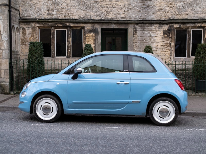
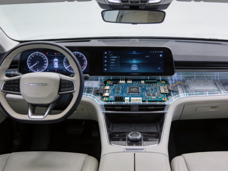
The automotive industry is undergoing a revolutionary transformation as vehicles evolve from simple transportation machines into sophisticated, intelligent systems. At the forefront of this evolution are Advanced Driver Assistance Systems (ADAS)—technologies that enhance vehicle safety, comfort, and performance through automated features like lane keeping, adaptive cruise control, and automatic emergency braking. Behind every ADAS feature lies a complex network of sensors, processors, and communication systems, all enabled by High Density Interconnect (HDI) Pcb Technology.
Hdi Technology has become the unsung hero of Automotive Electronics, providing the Miniaturization, reliability, and performance characteristics necessary for modern ADAS implementations. As vehicles integrate more sensors and computational power, HDI PCBs enable manufacturers to pack unprecedented functionality into limited space while meeting the rigorous demands of automotive environments. This comprehensive guide explores how Hdi Technology underpins ADAS systems and shapes the future of Automotive Electronics.

Understanding HDI Technology Fundamentals
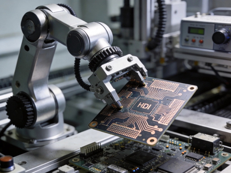
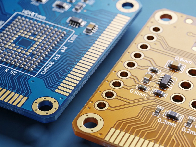
High Density Interconnect (HDI) technology represents a significant advancement in Pcb Manufacturing, enabling much higher component density than Traditional Pcb designs. Hdi Boards utilize Microvias, fine lines, and smaller capture pads to create more interconnects within a smaller footprint. The key characteristics that distinguish HDI technology include:
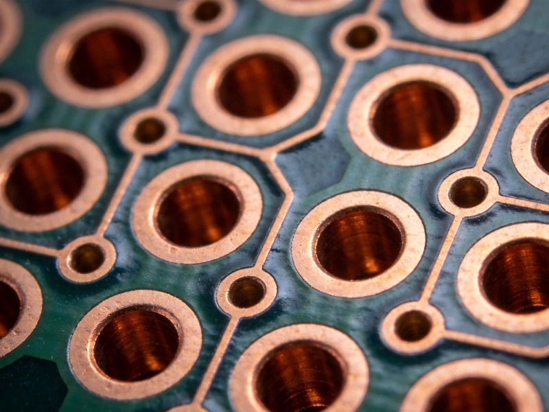
- Microvias: Laser-drilled holes with diameters typically less than 150 microns (6 mils) that create interconnections between layers without consuming the board space of traditional mechanically drilled vias. Microvias enable greater routing density and more efficient use of board real estate.
- Multiple Lamination Cycles: Hdi Boards often undergo Sequential Lamination processes, building up layers in stages to accommodate fine features and maintain reliability. This allows for more complex layer stack-ups and better control over impedance.
- Fine Line and Space: HDI technology supports trace widths and spacings as fine as 3 mils (75 microns) or less, compared to 5-6 mils for conventional boards. This enables higher routing density and more sophisticated circuit implementations.
- Smaller Capture Pads: Component pads can be reduced to match component dimensions, allowing more components per unit area. This Miniaturization is crucial for space-constrained automotive applications.
- Blind and Buried Vias: These vias connect only the layers needed without penetrating the entire board thickness, reducing space consumption and enabling more efficient routing strategies.
ADAS Systems and Their Electronics Requirements
Modern ADAS encompasses a diverse array of functions, each with specific electronics requirements that benefit from HDI technology:
- Camera Systems: Forward-facing, rear-view, and surround-view cameras require image sensors, processors, and communication interfaces—all packed into compact modules mounted in vehicle exteriors. HDI enables miniaturized camera control boards with high-speed video processing capabilities.
- Radar Systems: 77GHz and 24GHz radar sensors for adaptive cruise control and blind spot detection demand high-frequency Signal Integrity and precise Impedance Control. HDI technology provides the controlled impedance and low-loss dielectrics necessary for millimeter-wave signals.
- Lidar Systems: Light detection and ranging systems use rotating or solid-state arrays of laser emitters and detectors, requiring complex electronics in compact form factors. HDI enables the dense integration of laser drivers, detectors, and signal processing circuits.
- Ultrasonic Sensors: Parking assist systems use ultrasonic sensors distributed around the vehicle, each requiring local signal conditioning and communication interfaces. HDI allows miniaturized sensor modules with reliable performance.
- Control Units: Central ADAS processing units receive sensor data, perform fusion algorithms, and output control signals. These units require high-density memory arrays, multi-core processors, and complex interconnects—enabled by HDI technology.
Miniaturization Benefits for ADAS Applications
The automotive industry faces constant pressure to reduce vehicle weight and improve fuel efficiency while increasing electronic content. HDI technology addresses these challenges through dramatic miniaturization:
- Space Efficiency: ADAS sensors must often fit within tight vehicle constraints—side mirrors, bumpers, and interior trim panels. HDI technology reduces PCB size by 30-50% compared to conventional designs, enabling sensors to fit in available spaces without compromising functionality.
- Weight Reduction: Smaller PCBs use less material, contributing to overall vehicle weight reduction. In a typical modern vehicle with 30-40 electronic control units, the cumulative weight savings from HDI technology can be significant.
- Aesthetic Integration: Compact sensor modules can be integrated more seamlessly into vehicle styling, improving appearance while maintaining functionality. HDI enables sensors that are nearly invisible within vehicle exteriors.
- Multi-Function Modules: HDI allows combining multiple functions into single modules. A camera module might include image capture, processing, and communication interfaces on one compact board, reducing parts count and assembly complexity.
- Cost Optimization: While HDI boards have higher unit costs, the overall system cost often decreases due to reduced enclosure size, simplified assembly, and fewer interconnects between modules.
Signal Integrity and High-Speed Data Transmission
Modern ADAS systems transmit massive amounts of data—camera images, radar returns, lidar point clouds—at high speeds between sensors and processors. HDI technology provides the Signal Integrity necessary for these data-intensive applications:
- Controlled Impedance: Hdi Manufacturing enables precise control over trace impedance, critical for high-speed differential pairs used in video data transmission. Consistent impedance prevents signal reflections and maintains data integrity.
- Reduced Transmission Line Lengths: By enabling components to be placed closer together, HDI reduces trace lengths and associated signal degradation. This is particularly important for high-frequency signals used in radar and lidar systems.
- Low-Loss Dielectrics: HDI boards often use advanced dielectric materials with low dissipation factors, minimizing signal loss at high frequencies. This preserves signal quality for millimeter-wave radar and high-speed video.
- Differential Pair Routing: Fine line and space capabilities enable tighter coupling of differential pairs, improving common-mode rejection and electromagnetic compatibility—essential for reliable operation in the electrically noisy automotive environment.
- Crosstalk Mitigation: HDI technology's ability to route signals in dedicated layers with proper ground planes reduces crosstalk between adjacent signals, preserving data integrity in multi-sensor systems.
Thermal Management for High-Power ADAS Electronics
ADAS processors and radar transceivers generate significant heat, requiring effective Thermal Management strategies. HDI technology supports Thermal Management through several mechanisms:
- Thermal Vias: Dense arrays of Thermal Vias in HDI boards conduct heat from component junctions to inner ground planes or opposite board sides, improving Heat Dissipation without increasing board size.
- Inner Ground Planes: HDI's multiple layers provide dedicated ground planes that serve both electrical and thermal functions, spreading heat across the board and improving overall thermal performance.
- Copper Thickness Optimization: Hdi Manufacturing allows variable copper thicknesses within a board, using thicker copper for power and thermal planes while maintaining fine lines for signal routing.
- Component Placement Flexibility: The high routing density of HDI enables optimized component placement for thermal performance, positioning heat-generating components near thermal vias and heat sinks while maintaining electrical functionality.
- Material Selection: HDI technology accommodates advanced thermally conductive dielectric materials that improve heat transfer while maintaining electrical performance requirements.
Reliability Requirements for Automotive Applications
Automotive electronics must operate reliably for 10-15 years in harsh environments. HDI technology meets these demanding requirements through specific design and manufacturing approaches:
- Vibration Resistance: The smaller, more flexible traces in HDI boards are less susceptible to vibration-induced fatigue compared to larger traces in conventional boards. Component packages are also smaller and lighter, reducing vibration stress.
- Thermal Cycling Performance: HDI boards undergo rigorous thermal cycle testing to ensure reliability across the -40°C to +125°C temperature range experienced in automotive applications. Sequential Lamination processes create robust interconnects that withstand thermal expansion.
- Moisture Resistance: Advanced materials and manufacturing processes enable HDI boards to resist moisture ingress, crucial for exterior-mounted sensors exposed to rain, snow, and humidity. Conformal coating provides additional protection.
- Crosshatching for BGA Reliability: Under BGA components, HDI boards use crosshatched ground planes rather than solid planes, providing better thermal performance and reducing stress on solder joints during thermal cycling.
- Highly Accelerated Life Testing (HALT/HASS):strong> Automotive Hdi boards undergo extensive accelerated testing to validate reliability under combined stresses of temperature, vibration, humidity, and electrical loading.
Automotive Industry Standards and Compliance
HDI technology for ADAS applications must comply with rigorous automotive industry standards ensuring quality, reliability, and safety:
- AEC-Q100: The Automotive Electronics Council's AEC-Q100 standard defines stress test requirements for integrated circuits. HDI boards must accommodate component packages and interconnects that meet these requirements.
- IATF 16949: This automotive Quality Management System standard applies to Pcb Manufacturing facilities producing Automotive Hdi boards, ensuring consistent quality and continuous improvement.
- ISO 26262: Functional safety standard for automotive electrical and electronic systems. HDI boards used in safety-critical ADAS functions must support the design requirements for Automotive Safety Integrity Levels (ASIL).
- IPC-6012 Class 3: Electronics Industries Alliance standard for high-reliability electronic assemblies, specifying requirements for manufacturing, inspection, and testing. Automotive HDI boards typically require Class 3 compliance.
- VDA Standards: German automotive industry standards that supplement international requirements, particularly relevant for European automotive manufacturers.
HDI Technology in Specific ADAS Applications
Different ADAS functions leverage HDI technology in unique ways to achieve their performance goals:
- Forward Collision Warning: Systems using cameras and radar require precise timing and synchronization between sensors. HDI enables compact sensor modules with high-speed interfaces, supporting sensor fusion algorithms that detect potential collisions.
- Adaptive Cruise Control: Long-range radar sensors operating at 77GHz require HDI's controlled impedance and low-loss dielectrics for reliable millimeter-wave signal transmission. Miniaturized radar transceivers enable compact front grille integration.
- Lane Keeping Assist: Camera-based lane detection systems process high-resolution video in real-time. HDI enables compact camera control boards with multi-core processors and high-speed memory, mounted in windshield-mounted modules.
- Automatic Emergency Braking: This safety-critical function combines multiple sensors and rapid processing. HDI's reliability and high-density capabilities support redundant processing units and complex interconnects required for ASIL-D safety requirements.
- Parking Assist Systems: Surround-view cameras and ultrasonic sensors distributed around the vehicle require multiple compact sensor modules. HDI enables miniaturized electronics that fit in bumper cavities and side mirrors.
Integration Challenges and Solutions
Implementing HDI technology for ADAS presents specific challenges that require careful consideration:
- Design Complexity: HDI boards require specialized design expertise and sophisticated Pcb Design tools capable of handling microvias, sequential lamination, and complex layer stack-ups. Design teams need training in HDI-specific considerations.
- Manufacturing Cost: HDI boards are more expensive to manufacture than conventional boards due to laser drilling, multiple lamination cycles, and lower yields. However, system-level cost savings often offset this premium.
- Test and Inspection: Fine features in HDI boards challenge traditional inspection methods. Automated Optical Inspection (AOI) with enhanced capabilities and X-ray Inspection are required to ensure quality.
- Supply Chain Availability: Not all PCB manufacturers have HDI capabilities, especially for automotive applications requiring AEC-Q100 and ISO 26262 compliance. Careful supplier qualification is essential.
- Rework and Repair: Reworking HDI boards is more challenging than conventional boards due to microvias and dense component placement. Specialized processes and equipment are required for reliable rework.
Future Trends in HDI for ADAS
The evolution of ADAS systems continues to drive HDI technology innovation:
- Increased Layer Counts: Next-generation ADAS processors require more layers (12-16 or more) to accommodate increased functionality. HDI technology is evolving to support these high layer counts while maintaining reliability.
- Smaller Microvias: Advances in laser drilling technology enable microvias smaller than 100 microns (4 mils), increasing density and enabling even greater miniaturization of sensor modules.
- Any-Layer HDI: Any-layer HDI technology places microvias on every layer, maximum routing density and design flexibility. This approach enables more compact and sophisticated ADAS modules.
- Embedded Components: Embedding passive components within HDI board layers reduces component count and improves performance. This technology is gaining adoption in ADAS applications for sensor modules and control units.
- Advanced Materials: New dielectric materials with improved Thermal Conductivity, lower loss tangents, and better reliability are enabling higher performance HDI boards for next-generation ADAS systems.
The Role of HDI in Autonomous Driving
As vehicles progress toward higher levels of autonomy (Level 3, 4, and 5), HDI technology becomes increasingly critical:
- Increased Sensor Density: Autonomous vehicles require more sensors for comprehensive environmental perception. HDI enables the dense integration of multiple sensor types (cameras, radar, lidar) in compact modules.
- Enhanced Processing Power: Autonomous driving demands significant computational resources for sensor fusion, path planning, and decision making. HDI supports the high-density memory arrays and multi-core processors required for these tasks.
- Redundancy and Safety: Autonomous systems require redundancy for safety-critical functions. HDI enables compact redundant processing units and multiple sensor systems without excessive space consumption.
- High-Speed Communication: Inter-sensor and sensor-to-processor communication requires high-bandwidth, low-latency data links. HDI provides the signal integrity necessary for these high-speed interfaces.
- Power Distribution: The increased electronic content of autonomous vehicles requires sophisticated power distribution networks. HDI enables compact, efficient power management circuitry with high component density.
Manufacturing Considerations for Automotive HDI
Producing HDI boards for ADAS requires specialized manufacturing capabilities and processes:
- Laser Drilling: UV laser drilling systems create precise microvias with clean walls, essential for reliable plating and interconnection. Laser parameters must be carefully controlled for consistent results.
- Sequential Lamination: Multiple lamination cycles build up HDI boards layer by layer. Each cycle must be precisely controlled to maintain registration and prevent misalignment between layers.
- Desmear and Metallization: Microvias require specialized desmear and metallization processes to ensure reliable plating and electrical connection. The small via diameter makes these processes more challenging.
- Impedance Control: Tight impedance tolerances (±10% or better) are required for high-speed signals. This requires precise material selection and manufacturing process control.
- Quality Assurance: Comprehensive testing and inspection processes ensure reliability. This includes electrical testing, AOI, X-ray Inspection, and environmental testing for automotive qualification.
Cost-Benefit Analysis of HDI for ADAS
While HDI boards have higher unit costs, the total cost of ownership often favors HDI for ADAS applications:
- System-Level Cost Savings: Smaller PCBs reduce enclosure size, material usage, and assembly costs. Multiple functions can be integrated into single modules, reducing parts count and complexity.
- Performance Benefits: Improved signal integrity and thermal management enable higher performance ADAS functions, potentially commanding higher market prices or enabling premium features.
- Reliability Advantages: Better reliability reduces warranty costs and field failures, providing long-term cost savings despite higher initial board costs.
- Time-to-Market: HDI's design flexibility can accelerate development by enabling more functionality in smaller form factors, reducing mechanical design iterations.
- Scalability: HDI technology scales well to higher production volumes, with unit costs decreasing as processes mature and volumes increase.
Design Guidelines for ADAS HDI Boards
Successful HDI design for ADAS applications requires following specific guidelines:
- Layer Stack-Up Planning: Plan layer stack-up early, considering signal integrity, power distribution, and thermal management requirements. Include dedicated ground and power planes with adequate copper thickness.
- Microvia Placement: Position microvias strategically to maximize routing density while maintaining reliability. Avoid stacking microvias excessively—industry guidelines typically limit stacks to 2-3 microvias.
- Component Selection: Choose components with package sizes compatible with HDI capabilities. Prefer smaller packages (0402, 0201) for high-density areas, larger packages where rework is expected.
- Thermal Management: Include thermal vias under high-power components, use appropriate copper thicknesses for power planes, and consider component placement for optimal thermal performance.
- Design for Manufacturability: Work closely with your PCB manufacturer early in the design process to understand their specific HDI capabilities and design constraints. Follow their design rules and recommendations.
Testing and Validation of HDI ADAS Boards
Comprehensive testing ensures HDI boards meet automotive reliability requirements:
- Electrical Testing: Flying probe and bed-of-nails testing verify continuity, isolation, and impedance specifications. High-density boards may require specialized test fixtures.
- X-Ray Inspection: X-ray inspection examines Microvia quality, plating integrity, and solder joint quality under BGA components that aren't visible to optical inspection.
- Environmental Testing: Thermal cycling, temperature shock, humidity testing, and vibration testing validate reliability under expected operating conditions.
- Accelerated Life Testing: HALT and HASS testing identify potential failure modes and validate design margins before production commitment.
- In-Circuit Testing: Once populated with components, boards undergo ICT to verify component functionality and solder joint integrity before final assembly.
Conclusion
HDI technology has become an enabling technology for Advanced Driver Assistance Systems, providing the miniaturization, performance, and reliability necessary for modern automotive electronics. As ADAS capabilities continue to expand and vehicles progress toward higher levels of autonomy, HDI's role will only grow in importance. The technology's ability to pack unprecedented functionality into compact spaces while meeting the rigorous demands of automotive environments makes it indispensable for next-generation vehicle safety systems.
The investment in HDI technology pays dividends through improved performance, reduced system size and weight, enhanced reliability, and the ability to implement increasingly sophisticated ADAS features. For automotive manufacturers and suppliers, understanding HDI technology's capabilities and requirements is essential for competitive ADAS development.
As we look toward fully autonomous vehicles, HDI technology will continue evolving to support even greater sensor density, processing power, and communication bandwidth. The partnership between HDI technology and ADAS represents a powerful example of how advanced Electronics Manufacturing enables transformative automotive innovations that save lives, enhance comfort, and improve the overall driving experience.
FAQ
Q: What is the minimum microvia size used in automotive HDI boards?
A: Automotive HDI boards typically use microvias in the range of 100-150 microns (4-6 mils). Some advanced applications use microvias as small as 75 microns (3 mils), but smaller vias may present reliability challenges under automotive operating conditions. The minimum practical size depends on the PCB manufacturer's capabilities and the specific reliability requirements of the application.
Q: How many layers are typical in ADAS HDI boards?
A: ADAS HDI boards typically range from 8 to 16 layers, depending on functionality. Simple sensor modules might use 8-10 layers, while complex processing units with high-speed interfaces may require 12-16 layers. Layer count increases with functionality, power distribution requirements, and signal integrity considerations.
Q: Can HDI boards be reworked and repaired like conventional PCBs?
A: Yes, but rework is more challenging due to microvias and dense component placement. Specialized hot air rework stations, Precision Alignment systems, and skilled technicians are required. Rework success rates are lower for HDI boards compared to conventional boards, and design should account for rework challenges by providing adequate spacing and considering component replacement frequency.
Q: What are the typical cost differences between HDI and conventional PCBs?
A: HDI boards typically cost 30-100% more than conventional boards of similar size and layer count, depending on HDI features (microvia count, sequential lamination cycles) and production volume. However, system-level cost savings often offset this premium. At high volumes, the cost differential decreases as manufacturing processes mature and economies of scale are achieved.
Q: How do HDI boards handle automotive vibration requirements?
A: HDI boards meet automotive vibration requirements through several mechanisms: smaller, more flexible traces that resist vibration-induced fatigue; lighter component packages that reduce stress; robust plating processes that ensure reliable microvia connections; and compliance with AEC-Q100 component requirements. Additionally, HDI boards undergo extensive vibration testing during qualification to validate reliability.
Q: What environmental testing is required for automotive HDI boards?
A: Automotive HDI boards typically undergo multiple environmental tests: thermal cycling (-40°C to +125°C, hundreds of cycles), temperature shock, humidity testing (e.g., 85°C/85% RH for extended periods), vibration testing (sinusoidal and random), salt fog testing for exterior-mounted modules, and mechanical shock testing. Testing requirements are specified by automotive manufacturers and international standards.
Q: How does HDI technology impact ADAS time-to-market?
A: HDI can accelerate time-to-market by enabling more functionality in smaller form factors, reducing mechanical design iterations and integration complexity. However, HDI design is more complex and may require longer design cycles initially. Working with experienced HDI designers and manufacturers can mitigate this challenge and leverage HDI's benefits for faster development.
Are you developing ADAS systems and want to leverage HDI technology for optimal performance, miniaturization, and reliability? Partner with experienced Automotive Pcb manufacturers who understand the unique requirements of HDI boards for driver assistance systems and can help you achieve your design goals with confidence.