Open Nav

Thevia—the tiny copper-plated hole connecting layers in a printed circuit board—might seem like a simple feature. But in HDI (High-density Interconnect) manufacturing, how that via gets formed determines everything from board density to electrical performance to manufacturing cost. The choice between Laser Drilling and mechanical drilling isn't arbitrary; it reflects fundamental differences in capability, precision, and application suitability.
Over our years producing Hdi Boards from facilities across Guangdong and Jiangsu provinces, we've developed practical expertise in matching drilling methods to application requirements. The technical distinctions matter, but so do the practical realities of production capability, cost structures, and quality consistency that differ between methods.
This comparison cuts through marketing claims to examine what Laser Drilling and mechanical drilling actually deliver for HDI PCB Fabrication—and when each method makes sense for your design.
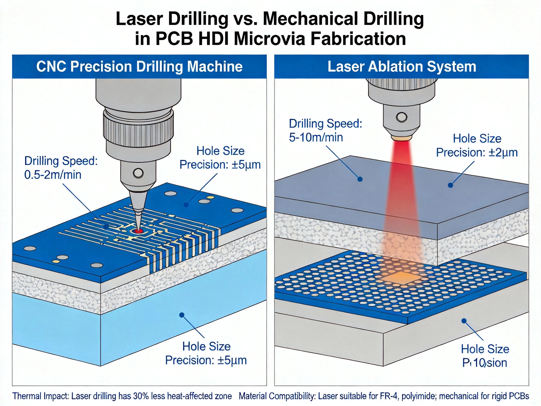
Mechanical drilling represents Traditional Pcb via formation. CNC-controlled drill bits cut through the substrate material physically, removing material through rotation and feed motion. This mature technology has produced billions of PCBs and remains the workhorse for via formation in standard and multilayer boards.
Mechanical drilling uses tungsten carbide or diamond-coated bits rotating at high speeds (typically 100,000-300,000 RPM) to cut through dielectric materials and copper layers. The drill bit diameter determines via size, with practical minimums around 0.15-0.20mm for standard production. Modern CNC drilling machines achieve positional accuracy of ±50μm, sufficient for through-hole vias and larger Blind Vias.
The drilling process creates thermal and mechanical stress on the substrate material. Entry and exit铜箔 surfaces require support to prevent burring and tear-out. Controlled-depth drilling for Blind Vias requires careful monitoring since the drill must stop precisely at the target layer without damaging underlying circuits.
Mechanical drilling excels for through-hole vias and larger blind vias (typically 0.30mm and above). The technology handles a wide range of board thicknesses and material types, including standard FR-4, high-Tg laminates, and metal-backed substrates. Setup is straightforward, and production costs scale favorably with volume.
However, mechanical drilling faces fundamental physical limitations. As drill bit diameter decreases, bit strength and lifespan decrease exponentially. Bits below 0.20mm become fragile, requiring slower feed rates and producing shorter tool life. Achieving consistent quality in small holes demands increasingly precise machine maintenance and environmental control. Aspect ratio limitations—depth-to-diameter ratios exceeding 10:1 create significant manufacturing challenges—constrain design flexibility for high-density boards.
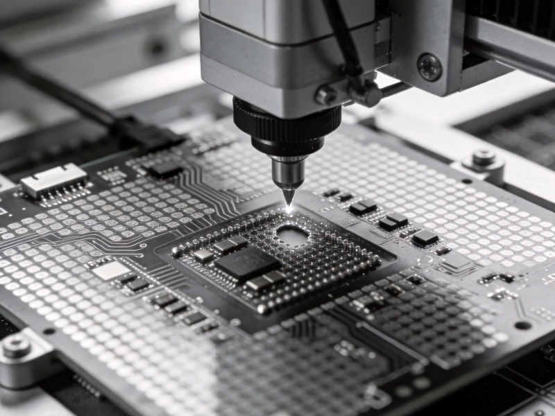
Laser drilling uses concentrated light energy to remove material, creating vias without physical contact. For Hdi Pcb Manufacturing, CO2 and UV laser systems have become essential tools for Microvia formation, enabling densities impossible with mechanical methods alone.
h3>Types of Laser Drilling SystemsCO2 lasers dominate PCB via formation, operating at infrared wavelengths (10.6μm) absorbed well by organic dielectric materials. These lasers vaporize substrate material layer-by-layer, creating tapered via walls with typical diameters of 50-150μm. CO2 laser systems can process an entire panel in seconds, making them highly productive for high-volume HDI production.
UV lasers operate at shorter wavelengths (355nm or 266nm) that interact differently with materials. UV ablation creates cleaner via walls with minimal heat-affected zones, making UV lasers preferred for sensitive substrates and ultra-fine features. However, UV systems offer slower processing speeds and higher operating costs than CO2 alternatives.
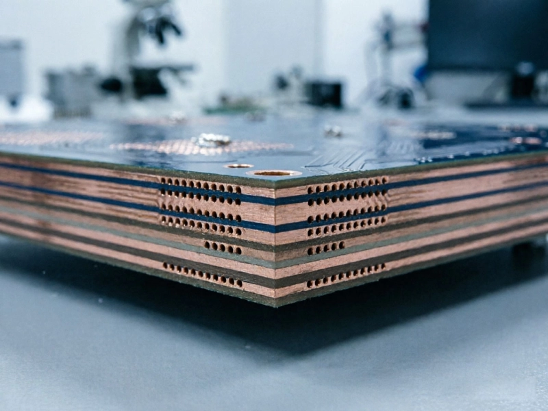
Laser drilling creates vias through sequential ablation—multiple pulses remove thin material layers until reaching the target depth. For Sequential Lamination HDI structures, laser processing occurs after each lamination cycle, drilling through the new dielectric layer to expose the underlying copper land. This "drill-as-you-go" capability enables complex layer stacking impossible with purely mechanical processing.
The laser's ability to target specific dielectric materials while leaving copper relatively unaffected enables unique structures. Laser ablation selectively removes prepreg or resin without attacking copper features, enabling precise controlled-depth processing for Blind Via formation.
Precision comparison reveals fundamental differences between the methods that directly impact design capability and manufacturing yield.
Mechanical drilling practically achieves minimum via diameters of 150-200μm, though some advanced facilities claim 100μm capability. This limitation stems from drill bit survivability and hole quality at extreme sizes. Laser drilling routinely produces 50-80μm vias, with advanced systems achieving sub-50μm features. This capability difference translates directly to achievable routing density—laser-drilled boards can pack more interconnects into smaller areas.
For typical smartphone applications requiring 0.4mm pitch BGA packages, laser Microvias are mandatory. Mechanical drilling simply cannot achieve the via densities and precise targeting that advanced packaging demands.
Modern CNC drilling achieves positional accuracy of approximately ±50μm (3-sigma), adequate for through-hole and larger Blind Via applications. Laser systems typically achieve ±25μm accuracy, with advanced systems claiming ±15μm. While both specifications seem small, the difference matters for fine-pitch components where via capture zones are minimized.
Stacked Microvia structures—where multiple microvia layers connect through Sequential Lamination—demand exceptional accuracy. Misalignment between laser-drilled layers compounds through the stack, requiring tight process control to maintain yield at acceptable levels.
Mechanical drilling creates rough hole walls with heat-affected zones that require desmear processing before plating. The drilling action compresses and redeposits material along hole walls, creating surface conditions that complicate uniform copper deposition. For high-reliability applications, mechanical via holes often require additional processing to ensure reliable plating adhesion.
Laser ablation creates smoother hole walls with minimal heat-affected zones, particularly for UV laser processing. The vaporization process produces cleaner surfaces that typically require less desmear treatment, potentially improving plating uniformity and reliability. However, laser-formed walls may exhibit different surface characteristics that require process adjustments for optimal plating results.
Material selection influences which drilling method proves most effective—and which combinations create unique manufacturing challenges.
Standard FR-4 materials respond well to both mechanical and laser processing. Mechanical drilling through FR-4 is straightforward, with predictable tool wear and consistent hole quality. Laser ablation of FR-4 creates characteristic tapered profiles that may require adjusted pad designs to accommodate geometry changes.
High-Tg FR-4 variants require consideration during laser processing—the higher glass transition temperature increases ablation energy requirements. Some facilities report reduced ablation efficiency for Tg values above 170°C, potentially affecting throughput and via quality.
PTFE-based substrates present unique challenges for mechanical drilling. The soft, compliant material tends to smear during drilling, requiring specialized techniques and tool geometries to achieve clean holes. Some facilities report significant quality issues when attempting mechanical drilling of pure PTFE materials, particularly at small diameters.
Laser drilling handles PTFE well, though the hydrophobic material requires surface preparation before desmear processing regardless of drilling method. The laser ablation process doesn't introduce the mechanical stress that causes PTFE smear, potentially producing cleaner holes with simpler post-processing requirements.
Modern HDI materials—resin-coated copper (RCC), laser-ablable prepregs, and specialized HDI laminates—are designed specifically for laser processing. These materials feature controlled dielectric constants, predictable ablation characteristics, and compositions optimized for sequential lamination processing. Using standard FR-4 for Hdi Applications may save material cost but often compromises manufacturing yield and final board performance.
Manufacturing cost structures differ significantly between drilling methods, influencing both pricing and production planning.
Mechanical drilling equipment ranges from $50,000 for basic CNC systems to $500,000+ for high-speed precision machines with automatic tool changing and vision systems. The capital requirement is substantial but spread across thousands of drill bits and many years of production.
Laser drilling systems command higher prices—professional CO2 laser drill systems range from $300,000 to over $1 million depending on capability and throughput. UV laser systems push toward the higher end, with associated operating costs for optics maintenance and consumables. This capital intensity concentrates laser capability in well-capitalized facilities capable of spreading investment across high-volume production.
Mechanical drilling costs depend heavily on drill bit consumption. Small diameter bits (below 0.25mm) have limited lifespan—sometimes only 100-500 holes before replacement. Tool cost per hole can exceed $0.01 for small holes, adding meaningful expense to high-density boards with thousands of vias. Larger holes become progressively cheaper as bits last longer and cost less per hole.
Laser processing costs include system depreciation, optics replacement, and processing time. While per-via costs are lower than mechanical drilling for small features, laser systems consume significant electricity and require maintenance downtime. For high-volume boards with many small vias, laser processing typically offers cost advantages despite higher equipment investment.
Manufacturing yield directly impacts effective cost. Mechanical drilling yield depends on drill bit consistency, machine maintenance, and material characteristics. Small-hole drilling shows higher scrap rates, with yield dropping as hole diameter decreases.
Laser drilling yields vary by via density and stack complexity. Stacked microvia structures require exceptional process control—any single layer failure causes board rejection. However, for standard staggered-via HDI designs, laser yields often exceed mechanical drilling yields for equivalent feature densities due to better consistency and process control.
Matching drilling method to application requirements optimizes both cost and performance. Here's a practical framework for decision-making.
Through-hole vias, large blind vias (0.30mm and above), and Buried Vias for multilayer boards favor mechanical drilling. Standard consumer electronics, industrial controls, and telecom equipment with moderate density typically achieve cost optimization with mechanical drilling throughout. Boards using standard materials without HDI requirements benefit from mechanical drilling's established process maturity and lower equipment overhead.
For designs with aspect ratios exceeding 8:1 or requiring non-standard board thicknesses, mechanical drilling provides flexibility that laser systems cannot match without specialized adaptation.
HDI structures with any-layer interconnection, fine-pitch components (0.5mm pitch and below), and high-density routing areas require laser microvia capability. Mobile devices, advanced computing hardware, and Medical Electronics typically mandate laser-drilled Microvias throughout. Any design targeting sequential lamination—where multiple HDI layers connect through stacked or staggered microvias—needs laser processing capability.
For applications demanding minimum board area or weight, laser-drilled microvia density enables designs impossible with mechanical methods.
Most HDI production uses both methods strategically. Standard through-hole and larger blind/Buried Vias form the board backbone mechanically, while fine-pitch areas and HDI layers use laser processing where required. This hybrid approach optimizes cost by reserving expensive laser processing for features that genuinely require it.
DFM analysis helps identify the optimal drilling method for each via in your design, potentially revealing opportunities to reduce manufacturing cost while maintaining required performance.
Both drilling technologies continue evolving, with developments likely to shift capability boundaries in coming years.
New tool coatings and geometries push mechanical drilling toward smaller diameters with better durability. Advanced machine designs achieve tighter positional accuracy and improved hole quality. However, fundamental physical limitations—the relationship between bit diameter, strength, and lifespan—resist breakthrough improvement.
Some facilities experiment with laser pre-ablation followed by mechanical finishing, combining technologies to overcome individual limitations.
Picosecond and femtosecond laser systems offer ultra-short pulses that create even cleaner ablation with minimal heat effects. These advanced systems remain expensive but continue penetrating high-end manufacturing. Direct imaging laser systems can potentially combine drilling and patterning functions, reducing total process steps.
Equipment cost declines as technology matures, gradually making advanced laser capability accessible to smaller facilities and lower-volume production.
Practical minimum for mechanical drilling is approximately 0.15-0.20mm diameter in production environments. Some facilities claim 0.10mm capability, but hole quality, positional accuracy, and manufacturing yield typically suffer at these extremes. For designs requiring smaller features, laser drilling is mandatory.
Yes, when properly processed. Laser Microvia Reliability depends on plating quality, surface preparation, and appropriate pad/via geometry design. Industry data shows Microvia Reliability often exceeds mechanically-drilled via reliability in Hdi Applications, primarily due to better hole wall quality and optimized HDI material systems designed for laser processing.
Cost optimization drives hybrid approaches. Mechanical drilling efficiently handles larger features (through-hole vias, large buried vias) that don't require laser precision. Laser processing handles fine features and HDI layer connections where only laser capability suffices. Using only laser processing for all vias would be unnecessarily expensive for features mechanical drilling handles adequately.
Via electrical characteristics depend more on geometry and plating quality than drilling method. Laser microvias often exhibit better high-frequency performance due to cleaner hole walls, more consistent plating, and materials optimized for laser processing. However, a poorly-designed laser microvia performs worse than a well-designed mechanical via for any given application.
Direct comparison is difficult since costs depend on via size, density, board complexity, and facility. Generally, laser microvia processing is cheaper than mechanical drilling for small features (below 0.25mm) due to lower tool consumption. For larger features, mechanical drilling is more economical. The comparison matters less than total manufacturing cost—laser-drilled boards often cost less overall when the design genuinely requires HDI capability.
Laser drilling and mechanical drilling serve different roles in HDI PCB Fabrication. Neither method dominates universally—optimal selection depends on your specific application requirements, density targets, and cost constraints.
For most standard and medium-density applications, mechanical drilling delivers adequate capability at favorable cost points. For advanced HDI applications requiring any-layer interconnection, fine-pitch component support, and maximum routing density, laser microvia capability is essential—and worth the associated manufacturing investment.
Understanding the tradeoffs helps you design boards that match manufacturing capability to application needs. Work with your fabricator early in design development to identify drilling method implications and optimize your design for both performance and manufacturing efficiency.
The technology continues evolving, with laser capability expanding and costs declining. Future HDI designs will likely leverage laser processing more extensively as the technology matures and penetrates broader production volumes.
The Challenge of Plating and Filling Microvias in HDI ProductionJuly/26/2026
Critical Quality Checkpoints in the HDI Production LineJuly/13/2026
How Manufacturers Achieve High Precision Alignment in 10+ Layer HDI BoardsAugust/15/2026
Overcoming Common Manufacturing Defects in High-Density InterconnectsSeptember/21/2026
Understanding Sequential Lamination in Multi-Step HDI BoardsJuly/03/2026
What is the Lead Time for Manufacturing Custom HDI Boards?October/12/2026
HDI Applications in Advanced Battery Management Systems (BMS)June/18/2026
HDI Solutions for High-Performance Gaming Consoles and LaptopsOctober/10/2026