Open Nav

High-density Interconnect (HDI) technology has revolutionized printed circuit board design by enabling unprecedented component density and signal performance. However, the sophisticated Microvias and complex plating structures that make HDI possible also introduce specific reliability challenges, with Plating Voids representing one of the most critical defects affecting interconnect integrity. Plating Voids—voids or gaps in the Copper Plating that lines vias and through-holes—can dramatically reduce current carrying capacity, create localized heating, and serve as initiation points for crack propagation under thermal cycling. Understanding the formation mechanisms, detection methods, and prevention strategies for plating voids is essential for anyone involved in Hdi Pcb design, fabrication, or quality assurance.
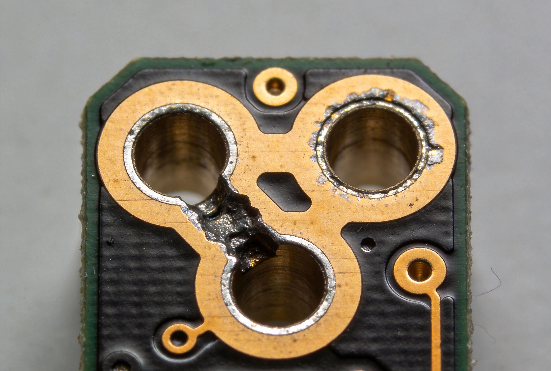
Plating voids are discontinuities in the Copper Plating that coats the internal surfaces of vias, through-holes, and blind/Buried Vias in PCBs. These voids range from microscopic imperfections barely detectable with high-magnification inspection to substantial gaps that significantly reduce the effective copper cross-section available for current flow.
Plating voids manifest in several distinct forms, each with different formation mechanisms and reliability implications. Understanding these types helps in identification, prevention, and risk assessment.
Gas Bubble Voids: Perhaps the most common type, gas bubble voids form when gas bubbles become trapped during plating and prevent copper deposition in the affected area. These typically appear as spherical or elliptical voids, often located in the upper portion of vias where bubbles naturally rise. The size varies from microscopic to substantial depending on bubble size and plating conditions.
Entrapment Voids: These occur when debris, particles, or contaminants become trapped in the via during drilling or cleaning and block copper deposition. Entrapment voids often have irregular shapes reflecting the geometry of the trapped material. These are particularly problematic because they may not be apparent from external inspection but create significant reliability risks.
Shadowing Voids: Shadowing occurs when features in the via geometry or adjacent structures prevent uniform current distribution during plating, resulting in areas with insufficient plating. These often appear in complex via geometries, stacked via structures, or areas with dense via arrays where current distribution becomes non-uniform.
Wetting Voids: These occur when the plating solution does not properly wet the via surfaces, often due to surface contamination, inadequate cleaning, or surface energy issues. Wetting voids typically appear as coating defects rather than discrete voids, creating thin or patchy plating coverage.
Cracking Voids: These form when plating develops micro-cracks during processing or subsequent thermal cycling. The cracks can propagate and create voids over time, particularly under thermal stress. Cracking voids represent a progressive failure mechanism that may not be apparent immediately after fabrication.
The location of plating voids within the interconnect structure significantly affects reliability. Voids in different positions create different stress concentrations and failure modes.
Voids at the via barrel wall are particularly problematic because they directly reduce current carrying capacity and create stress concentration points where cracks can initiate. These voids are especially critical in current-carrying vias where electrical performance is paramount.
Voids at the via pad interface affect the transition between the via barrel and the copper pad, creating impedance discontinuities and potential failure points. This location is particularly sensitive because it experiences mechanical stress during thermal cycling and soldering processes.
Voids in stacked via structures represent multiple failure points in series. Each void increases overall resistance and creates stress concentration points. In these complex structures, the interaction between multiple voids can accelerate failure progression.
Voids in Microvias are especially concerning because the small size of microvias means that even relatively small voids represent a substantial percentage of the available cross-section. Microvias also experience higher current density and thermal stress due to their smaller dimensions, making them more vulnerable to void-related failures.
Not all plating voids have equal impact on reliability. Void size, location, and quantity all contribute to overall risk assessment. Industry standards and quality specifications typically establish acceptance criteria based on these factors.
Microscopic Voids: Voids smaller than 10-20% of the via diameter typically have minimal impact on current carrying capacity but may serve as stress concentration points. These are often acceptable in less critical applications but may warrant rejection in high-reliability applications.
Moderate Voids: Voids ranging from 20-50% of the via diameter represent significant reductions in current carrying capacity. These voids create substantial stress concentrations and often exceed acceptance criteria for most applications.
Severe Voids: Voids larger than 50% of the via diameter dramatically reduce interconnect capability and typically represent immediate reliability concerns. These voids almost always exceed acceptance standards and require board rejection or rework.
Multiple Voids: The presence of multiple voids, even if individually moderate, compounds reliability risks. The interaction between multiple voids can create cumulative effects greater than the sum of individual impacts.
Understanding how plating voids form is essential for developing effective prevention strategies. Voids can originate at various stages of the PCB Fabrication process, with each stage presenting different risk factors and control opportunities.
The drilling process represents the first opportunity for void formation to begin. Several drilling-related issues can create conditions that lead to plating voids during subsequent plating operations.
Drill Bit Wear: Worn drill bits create rough, irregular hole surfaces that may trap debris or create shadows that prevent uniform plating. The roughness also increases surface area, requiring longer plating times to achieve adequate coverage. Drill bit wear should be monitored through hole quality inspection and drill bit replacement schedules.
Debris Generation: Drilling generates substantial debris that must be thoroughly removed before plating. Incomplete debris removal results in particles that become trapped during plating and create entrapment voids. Debris removal processes including mechanical desmearing, chemical etching, and cleaning must be carefully controlled.
Smear Formation: The drilling process can create a smear layer of resin and copper on the hole walls. This smear must be removed through desmearing processes to ensure proper plating adhesion. Incomplete desmearing creates surface contamination that prevents proper plating wetting and can lead to void formation.
Geometry Defects: Drilling defects including out-of-round holes, taper, or bellmouth effects create non-uniform geometries that affect plating current distribution. These geometry defects can create shadowing effects where certain areas receive insufficient plating current, resulting in thin plating or voids.
Proper surface preparation is critical for achieving uniform copper plating. Deficiencies at this stage directly contribute to plating voids and other coating defects.
Insufficient Cleaning: Contaminants including oils, residues, or particles remaining on via surfaces prevent proper copper plating. Cleaning processes must remove all contaminants while maintaining surface properties conducive to plating adhesion. Cleaning solution composition, temperature, and exposure time all affect cleaning effectiveness.
Surface Activation Issues: Plating requires properly activated surfaces to initiate copper deposition. Inadequate activation results in patchy or incomplete plating. Activation bath composition, concentration, and dwell time must be optimized for specific materials and geometries.
Roughness Control: Surface roughness affects plating uniformity and adhesion. Excessive roughness can trap debris and create shadowing effects. Insufficient roughness reduces adhesion strength. Optimal roughness depends on material properties and plating requirements.
The plating process itself offers multiple opportunities for void formation through parameter control and process variability. Precise control of plating conditions is essential for minimizing voids.
Current Distribution: Non-uniform current distribution during plating creates shadowing effects where certain areas receive insufficient plating current. This is particularly problematic in dense via arrays or complex geometries. Pulse plating, optimized anode placement, and bath agitation help improve current uniformity.
Gas Evolution: Electroplating generates hydrogen gas at the cathode surface. If this gas cannot escape from tight geometries quickly enough, bubbles become trapped and create voids. Bath chemistry, current density, and agitation rate affect gas evolution and removal.
Bath Chemistry: Plating bath composition including brighteners, levelers, and wetting agents significantly affects plating quality and void formation. Improper bath chemistry can cause excessive gas generation, poor throwing power, or other defects that contribute to voids. Bath chemistry must be regularly monitored and maintained.
Temperature Control: Plating temperature affects solution viscosity, reaction rates, and gas solubility. Temperature variations lead to inconsistent plating results. Precise temperature control within tight tolerances is essential for consistent plating quality.
Filtration Issues: Particulates in plating solutions can become trapped in vias and create entrapment voids. Effective filtration with appropriate pore size ratings removes particulates while preserving bath chemistry. Filter maintenance and replacement schedules prevent filter degradation that could release particles.
The materials used in PCB construction and plating influence void formation through their interaction with plating processes.
Dielectric Material Properties: Different dielectric materials have varying surface energies, wettability, and interaction with plating chemistry. Some materials require specialized surface treatments or modified plating parameters to achieve proper plating coverage.
Copper Foil Quality: The quality of initial copper foil affects subsequent plating processes. Surface roughness, contamination, or oxidation on foil surfaces can propagate through multiple processing steps and contribute to void formation.
Material Interactions: Different materials in the stackup may respond differently to plating processes, creating differential plating rates or adhesion issues. These material interactions must be considered when developing plating processes for complex stackups.
Plating voids create multiple reliability risks that can lead to field failures, particularly in demanding applications with high current, thermal cycling, or long service life requirements.
The most immediate impact of plating voids is reduction of available copper cross-section for current flow. The current carrying capacity of a via depends on the minimum cross-sectional area along its length. Voids reduce this minimum cross-section, creating bottlenecks where current density becomes excessive.
Current density increases inversely with cross-sectional area. A void reducing the effective cross-section by 50% doubles the current density in the remaining copper. Since heating in conductors follows P = I²R, the heating at the voided location increases dramatically. This localized heating can create thermal stress, accelerate material degradation, and potentially lead to thermal runaway in extreme cases.
In high-current applications, this reduction in current carrying capacity can be the difference between reliable operation and premature failure. Design margins that account for normal variations in plating thickness may be insufficient when voids are present.
Plating voids affect Thermal Performance in multiple ways. The reduced copper cross-section decreases Thermal Conductivity along the via, reducing its ability to conduct heat between board layers. This is particularly important in Thermal Vias designed to conduct heat from hot components to opposite board surfaces.
Voids also create thermal discontinuities where heat transfer is interrupted. These thermal hot spots create temperature gradients that stress adjacent materials and solder joints. The temperature differentials can also create thermomechanical stress that accelerates crack formation and propagation.
In applications with high power density or demanding thermal requirements, the Thermal Performance degradation from plating voids can compromise overall system Thermal Management, leading to component overheating and reduced reliability.
Plating voids create geometric discontinuities that act as stress concentration points under thermal or mechanical loading. During thermal cycling, different materials in the PCB stackup expand and contract at different rates, creating shear stresses at material interfaces.
Voids serve as initiation points for crack formation in the copper plating. Once a crack initiates, it can propagate through repeated thermal cycling, eventually severing electrical connectivity. This failure mechanism is particularly insidious because it may not be detectable immediately after fabrication but manifests after the device has been in service.
The stress concentration effect is magnified by the thermal cycles themselves. Each thermal cycle fatigues the copper plating, with voids acting as stress amplifiers. Boards with plating voids may appear functional initially but fail after thousands or millions of thermal cycles.
In high-speed or high-frequency applications, plating voids create electrical discontinuities that affect Signal Integrity. The abrupt change in conductor geometry creates impedance mismatches that cause signal reflections and distortion.
The reduced cross-section increases via resistance, creating voltage drops and potentially affecting power distribution in power-carrying vias. In differential signal pairs, asymmetric voiding can create impedance imbalances that degrade signal quality.
For signals operating at frequencies where via inductance and resistance matter, voids can create unpredictable variations in electrical characteristics. This variability makes board design and Signal Integrity simulation less reliable when voids are present.
Plating voids accelerate aging mechanisms and reduce overall board service life. The elevated temperatures, stress concentrations, and reduced material volume all contribute to accelerated degradation compared to vias without voids.
This accelerated aging is particularly problematic in applications requiring long service lives such as aerospace, automotive, or industrial equipment. A board designed for a 20-year service life may fail much earlier when plating voids are present, compromising system reliability and creating maintenance or replacement costs.
Effective detection of plating voids is essential for Quality Control and reliability assurance. Various inspection methods exist, each with capabilities and limitations.
X-ray Inspection is the most common method for detecting plating voids in assembled boards and prototype samples. X-rays penetrate the board materials and reveal internal structures, including via plating quality.
2D X-Ray: Conventional 2D X-ray provides shadow images that reveal voids as lighter areas within the via plating. This method is widely available and provides good detection of large voids but may miss small voids or provide ambiguous results due to overlapping structures.
3D Computed Tomography (CT): 3D CT scanning provides volumetric images that allow detailed analysis of plating quality throughout the via volume. This method provides the most comprehensive void detection but requires more expensive equipment and longer scan times. It is typically used for detailed analysis rather than routine inspection.
X-ray Inspection advantages include Non-destructive Testing, ability to inspect boards after assembly, and detection of internal defects. Limitations include difficulty detecting small voids in complex geometries, limited resolution for very fine features, and equipment cost.
Cross-section analysis involves cutting through vias and examining the exposed plating under microscopy. This destructive method provides detailed information about plating quality and is often used for process qualification and failure analysis.
Sample Selection: Representative samples are selected for cross-sectioning based on production lots, defect analysis, or quality monitoring requirements. The sampling method significantly affects the statistical validity of the results.
Preparation: Cross-section preparation involves careful cutting, mounting, polishing, and etching to reveal the via structure without introducing artifacts. Poor preparation can create misleading results or mask actual defects.
Analysis: Microscopic examination at various magnifications reveals plating thickness, void presence, and other quality parameters. Advanced analysis including SEM (scanning electron microscopy) can reveal micro-structural details.
Cross-section advantages include detailed analysis, absolute measurement capability, and ability to examine multiple vias in a single sample. Disadvantages include destructive nature, labor-intensive preparation, and statistical limitations from small sample sizes.
Electrical testing provides indirect evidence of plating voids through measurements of electrical characteristics. While not a direct void detection method, electrical testing can flag suspicious vias for further inspection.
Resistance Measurement: Elevated resistance in vias indicates potential plating issues including voids. However, resistance can be affected by multiple factors, making definitive void diagnosis difficult from resistance alone.
Continuity Testing: Opens detected during continuity testing may result from plating voids that have propagated into complete failures. However, continuity testing typically only detects catastrophic failures, not partial voids.
Current Carrying Testing: Testing vias under load can reveal thermal issues that might result from voids. Elevated temperature rise under load suggests reduced cross-section potentially caused by voids.
Electrical testing advantages include non-destructive nature, ability to test all vias, and relatively low cost. Limitations include indirect evidence and inability to definitively identify voids as the cause of observed effects.
Visual inspection of open vias and through-holes can reveal surface defects that may indicate underlying plating issues. While limited to surface examination, visual inspection provides quick feedback on obvious problems.
Optical Microscopy: High-magnification optical examination of via openings reveals surface plating quality, discoloration, or other visible defects. Some voids may be visible at the via opening if they extend to the surface.
Borescope Inspection: Internal borescopes allow visual inspection of via interiors without cross-sectioning. This method is particularly useful for deep holes or complex geometries.
Visual inspection advantages include quick results, low cost, and ability to inspect all vias. Limitations include surface-only examination and difficulty seeing internal voids unless they extend to the surface.
In-process monitoring tracks plating process parameters and provides early warning of potential void issues before boards are completed.
Bath Analysis: Regular chemical analysis of plating bath composition ensures proper chemistry that supports quality plating and minimizes void formation.
Current Monitoring: Monitoring plating current distribution and patterns helps identify potential shadowing or uniformity issues that could lead to voids.
Thickness Measurement: Plating thickness measurement on test coupons provides ongoing verification that plating thickness meets specifications and indicates potential process issues.
In-process monitoring advantages include early problem detection, prevention of defective lots, and process control data. Limitations include indirect correlation with actual void formation and the need for sophisticated monitoring equipment.
Preventing plating voids requires attention to multiple process steps and implementation of robust control measures. Effective prevention combines process optimization, Quality Control, and continuous improvement.
The drilling process sets the foundation for quality plating. Optimizing drilling parameters reduces debris generation, improves hole quality, and creates surfaces conducive to uniform plating.
Drill Bit Management: Implement systematic drill bit replacement based on hole count or hole quality metrics rather than arbitrary time intervals. Track drill bit performance through quality metrics to optimize replacement schedules.
Parameter Optimization: Optimize drill speed, feed rate, and peck cycles for specific materials and hole sizes. Different materials and hole geometries require different drilling parameters to minimize debris and hole wall defects.
Vacuum Systems: Effective vacuum chip removal systems prevent debris accumulation in holes during drilling. Regular maintenance of vacuum systems ensures consistent debris removal performance.
Cooling and Lubrication: Proper cooling and lubrication reduces heat generation and prevents resin melting that creates smear. Optimized coolant application maintains consistent hole quality across the drilling process.
Thorough cleaning and desmearing removes debris and smear that could lead to void formation. These processes must be optimized for specific materials and hole geometries.
Chemical Desmearing: Optimize desmearing chemistry, temperature, and dwell time for specific dielectric materials. Over-desmearing can roughen surfaces, while under-desmearing leaves smear that impedes plating.
Ultrasonic Cleaning: Ultrasonic agitation improves cleaning effectiveness, particularly in small, deep holes where mechanical cleaning is less effective. Parameters including frequency and power must be optimized to avoid damage.
Rinse Water Quality: High-purity rinse water prevents contamination that could affect subsequent plating. Regular water quality monitoring ensures rinse effectiveness.
Drying Processes: Effective drying prevents water spots or residues that could interfere with plating. Proper drying temperature and airflow are essential.
Precise control of plating parameters minimizes void formation. Process control extends beyond basic parameter settings to include ongoing monitoring and adjustment.
Pulse Plating: Pulse plating with appropriate current profiles improves throwing power and reduces gas bubble entrapment. Pulse parameters including on-time, off-time, and current density must be optimized for specific geometries.
Bath Agitation: Proper bath agitation ensures uniform solution composition and temperature, removes gas bubbles, and improves plating uniformity. Agitation method and intensity must be optimized for specific via geometries.
Anode Configuration: Optimized anode placement improves current distribution and reduces shadowing effects. For complex boards with dense via arrays, auxiliary anodes may be necessary to achieve uniform plating.
Temperature Control: Tight temperature control within ±1°C ensures consistent plating reaction rates and solution viscosity. Precise temperature control requires properly calibrated controllers and adequate Thermal Management systems.
Filtration Systems: Multi-stage filtration with appropriate pore size ratings removes particulates that could create entrapment voids. Regular filter maintenance and replacement prevent filter degradation and particle release.
Appropriate material selection and preparation supports quality plating and reduces void formation risk.
Dielectric Material Selection: Select dielectric materials with proven compatibility with plating processes. Some materials require specialized surface treatments or modified plating parameters.
Surface Activation Optimization: Optimize activation processes for specific materials. Activation chemistry, concentration, and dwell time significantly affect plating adhesion and uniformity.
Copper Foil Quality: Use high-quality copper foil with consistent surface properties. Verify foil quality through incoming inspection and supplier qualification processes.
Robust quality assurance processes ensure that plating quality meets specifications and that process issues are identified and addressed before they create defective boards.
Statistical Process Control: Implement statistical process control on critical parameters including plating thickness, resistance, and visual inspection results. Control charts and capability studies provide ongoing visibility into process performance.
First Article Inspection: Comprehensive inspection of first articles from each lot or production run establishes baseline quality and prevents production of defective lots.
Lot Acceptance Testing: Implement lot acceptance testing based on risk assessment and application requirements. Testing may include electrical testing, X-ray inspection of sample boards, or cross-section analysis of test coupons.
Failure Analysis Protocols: Establish protocols for investigating defects when they occur. Systematic failure analysis identifies root causes and enables preventive action.
Design choices can influence susceptibility to plating void failures and affect how voids impact reliability. Design for manufacturing considerations can reduce void-related risks.
Via geometry affects plating quality and void susceptibility. Design choices that improve plating uniformity reduce void formation risk.
Aspect Ratio: Maintain reasonable aspect ratios to ensure uniform plating current distribution. Very high aspect ratios create plating challenges that increase void risk. Consider alternative routing strategies when high aspect ratios are required.
Via Placement: Distribute vias to avoid extremely dense arrays where current uniformity becomes challenging. Maintain minimum spacing between vias to allow uniform plating current distribution.
Via Size Standardization: Standardize via sizes where possible to simplify plating process optimization. Multiple via sizes with very different aspect ratios complicate plating parameter optimization.
Design with adequate current capacity margins accounts for potential plating voids and provides reliability buffer.
Current Derating: Apply appropriate current derating factors to vias based on application criticality and manufacturing process capability. Derating accounts for expected variations in plating quality including potential voids.
Via Redundancy: Where possible, use multiple vias in parallel for critical current paths. Redundancy provides fault tolerance if one via has plating issues.
Larger Vias: Use larger vias where space allows. Larger vias provide greater plating surface area and are less affected by small voids as a percentage of total cross-section.
Thermal design that accounts for potential plating voids reduces reliability risk from thermal performance degradation.
Thermal Via Arrays: Use arrays of Thermal Vias rather than relying on single vias for critical thermal paths. Redundancy provides fault tolerance for plating voids.
Conservative Thermal Design: Design for thermal performance with appropriate margins. Conservative design provides buffer against thermal degradation that might result from plating voids.
Design for testability and inspectability improves ability to detect plating voids and assess reliability.
Test Via Inclusion: Include test vias that are not electrically required but allow convenient inspection of plating quality. Test vias can be cross-sectioned for detailed analysis without sacrificing production vias.
Access for Inspection: Design board layouts that provide access for X-ray inspection of critical vias. Avoid placing components or other features that block X-ray inspection of important vias.
Industry standards provide guidelines for acceptable plating quality and help establish consistent expectations across the supply chain.
IPC (Association Connecting Electronics Industries) publishes standards covering PCB Fabrication including plating quality requirements.
IPC-6012: Standard for rigid Pcb Fabrication includes requirements for plating quality, via plating thickness, and acceptable defect levels including voids.
IPC-6013: Standard for flexible Pcb Fabrication addresses plating quality requirements specific to flexible circuits.
IPC-600: Acceptability of printed boards provides visual inspection criteria for various defect types including plating issues.
Certain industries have more stringent requirements driven by application-specific reliability needs.
Automotive Standards: Automotive Electronics standards including Aec-q100 and Iatf 16949 impose strict quality requirements on plating and interconnect reliability.
Aerospace Standards: Aerospace standards including MIL-PRF-31032 and ESA requirements specify comprehensive quality and reliability requirements for PCBs used in space applications.
Medical Standards: Medical Electronics standards including IEC 60601 require particularly high reliability for life-critical applications.
Plating voids represent a significant reliability concern in Hdi Pcb interconnects, affecting electrical performance, thermal management, mechanical integrity, and overall service life. Understanding the formation mechanisms, detection methods, and prevention strategies is essential for anyone involved in Hdi Pcb Design, fabrication, or quality assurance.
Effective management of plating void risks requires attention throughout the fabrication process, from drilling and surface preparation through plating and final inspection. Prevention through process optimization, detection through appropriate inspection methods, and mitigation through design margins all contribute to reliable HDI products.
As Hdi Technology continues to advance with increasingly complex Microvia structures and higher density requirements, the importance of managing plating void risks will only increase. Manufacturers that develop robust capabilities in plating Void Prevention, detection, and management will be well-positioned to meet the demanding reliability requirements of next-generation electronic products.
The complexity of HDI structures means that some plating voids are inevitable despite best prevention efforts. The goal is not zero voids but rather effective management of void risk through comprehensive prevention, detection, and design for resilience strategies. When properly managed, plating voids need not compromise the reliability that Hdi Technology enables.
Most plating voids result from gas bubbles becoming trapped during plating, debris entrapment from drilling or cleaning processes, or poor plating current distribution that creates shadowing effects. Process parameter variations including bath chemistry, temperature, and agitation also contribute. Proper control of drilling, cleaning, and plating processes addresses the majority of void formation causes.
X-ray inspection is the primary non-destructive method for detecting plating voids. 2D X-ray can reveal larger voids, while 3D CT scanning provides detailed volumetric analysis. Electrical testing including resistance measurements can indirectly indicate potential void issues. For comprehensive quality control, combine X-ray inspection with cross-section analysis of representative samples from production lots.
Acceptable void size depends on application criticality and via geometry. Generally, voids smaller than 10-20% of the via diameter are acceptable in less critical applications. Voids larger than 50% typically exceed acceptance standards for most applications. Application-specific standards may have more stringent requirements. High-reliability applications typically require more conservative void acceptance criteria.
Repair is typically impractical once a board is complete, though techniques exist for reworking specific vias in some cases. The primary approach is prevention through process control and detection through inspection to prevent defective boards from reaching assembly. When voids are discovered in production lots, process improvements prevent recurrence in future lots.
Plating voids create impedance discontinuities that cause signal reflections and distortion in high-speed applications. The abrupt change in conductor geometry affects both resistance and inductance of the via. In differential pairs, asymmetric voiding can create impedance imbalances that degrade signal quality. For very high-frequency signals, even small voids can affect signal integrity.
Reliability Challenges of Via-in-Pad Plating Filled (VIPPO) TechnologySeptember/30/2026
The Impact of HDI on LiDAR and Radar Sensor PerformanceOctober/15/2026

The Role of IPC Standards in HDI PCB Quality AssuranceSeptember/08/2026
Conductive Anodic Filament (CAF) Resistance in High-Density BoardsJuly/31/2026
Understanding and Preventing Microvia Cracking in Thermal CyclingJune/12/2026
How HDI Technology Enables the Miniaturization of Modern ElectronicsSeptember/20/2026
Understanding Sequential Lamination in Multi-Step HDI BoardsJuly/03/2026

The Evolution of PCB Technology: From Standard Multilayer to HDIJune/02/2026