Open Nav

The fifth generation of wireless technology represents more than just faster data speeds for mobile devices. 5G networks demand fundamental changes in infrastructure, from antenna arrays to backhaul equipment, and nowhere are those changes more visible than in the circuit boards that power base stations. The combination of high-frequency operation, dense component placement, and harsh environmental requirements forces base station PCB designers to rely on advanced materials that standard FR-4 simply cannot deliver.
High Density Interconnect (HDI) technology with low-loss materials has emerged as the enabling solution for 5G base station requirements. This guide explores why these materials matter, what makes them different from standard PCB substrates, and how manufacturers and designers are leveraging them to build the next generation of wireless infrastructure.
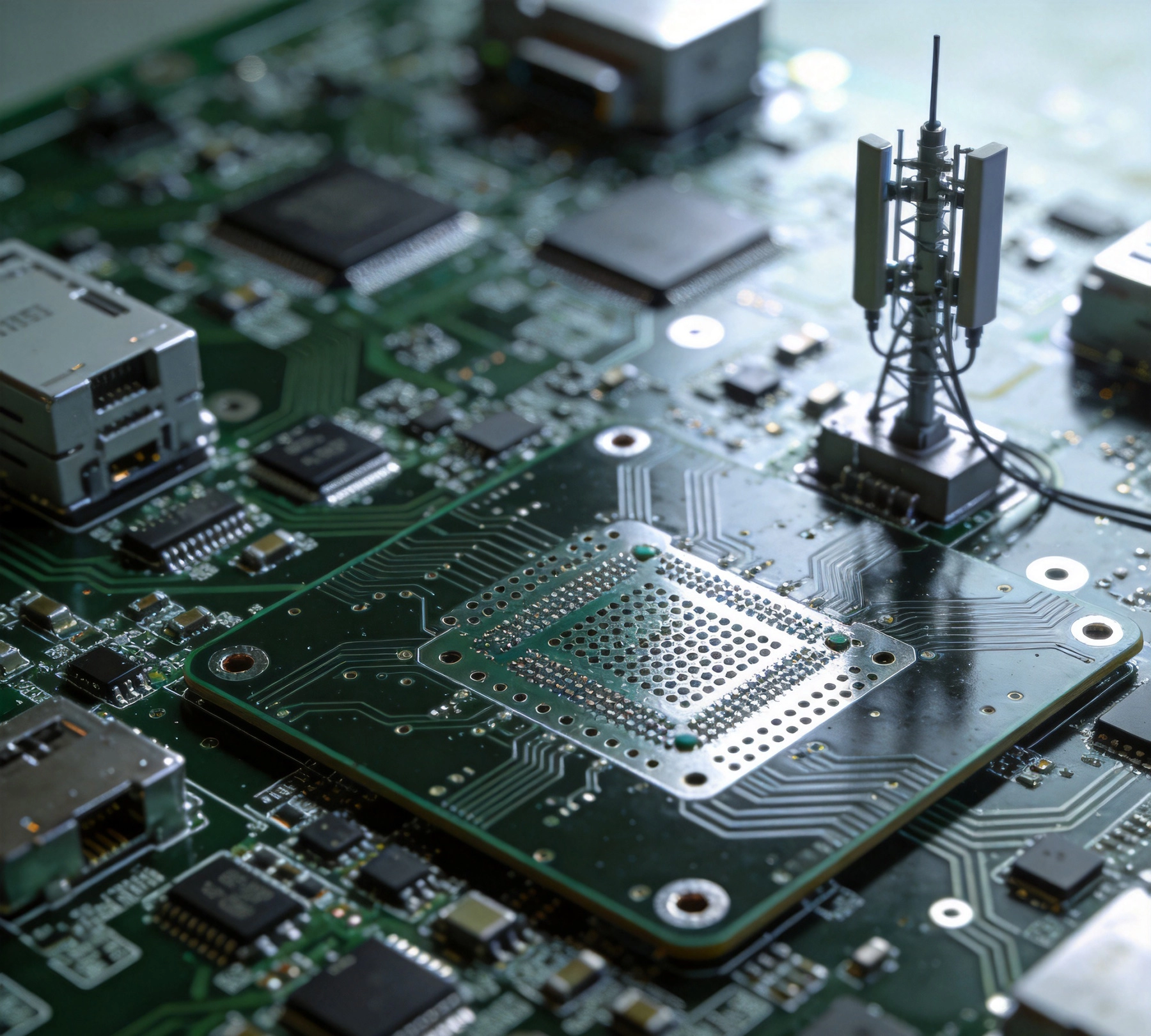
5G operates across a dramatically different frequency spectrum than 4G networks. While 4G LTE primarily uses frequencies below 3 GHz, 5G spans from sub-6 GHz bands up to millimeter-wave frequencies around 28 GHz and even 39 GHz in some implementations. This frequency shift changes everything about signal propagation, attenuation, and the materials needed to support reliable transmission.
At these frequencies, signal loss becomes a critical design constraint. Every millimeter of trace, every via transition, and every material interface introduces signal attenuation. In 4G systems, loss might be manageable with standard materials and design techniques. In 5G, that same loss could render a design unworkable or require unacceptable power amplification to compensate. This is why low-loss materials have moved from specialized applications to mainstream requirements for 5G infrastructure.
High Density Interconnect technology enables component placement densities that traditional Pcb Manufacturing cannot achieve. Through Microvias, blind and Buried Via structures, and fine-line trace widths, HDI PCBs pack components more tightly while maintaining or improving Signal Integrity. For 5G base stations, this density matters for several reasons.
First, 5G antenna arrays require massive MIMO (Multiple-Input Multiple-Output) configurations with dozens or even hundreds of antenna elements arranged in precise patterns. Each element needs its own signal path, power conditioning, and control circuitry. Standard PCB processes cannot provide the interconnection density required for these arrays without making boards impossibly large or layer counts unmanageable. Hdi Technology with Microvias provides the routing density needed to fit these complex signal paths in form factors suitable for rooftop or pole-mounted installations.
Second, base station form factors continue shrinking despite increased functionality. Network operators want smaller, lighter equipment that reduces installation costs and simplifies deployment in urban environments. Hdi Technology enables board size reduction without sacrificing functionality or reliability, which is critical for meeting these packaging goals.
Microvias, with diameters typically below 150 microns, enable vertical interconnections between layers with minimal parasitic inductance and capacitance. For high-frequency signals, this matters because every via transition creates signal reflections and impedance discontinuities. Smaller vias reduce these parasitic effects, making them essential for maintaining Signal Integrity at multi-gigahertz frequencies.
Standard through-hole vias act as stubs that create signal reflections and require careful back-drilling to remove unused barrel portions. Blind and buried microvias eliminate this problem entirely by providing direct layer-to-layer connections without stubs. The result is cleaner signal transmission and more predictable high-frequency performance.
The two most critical material parameters for high-frequency PCB performance are dielectric constant (Dk) and dissipation factor (Df). Standard FR-4 has a Dk around 4.5 and a Df around 0.02, which works adequately at lower frequencies but becomes problematic above a few gigahertz. Low-loss materials typically feature Dk values between 2.8 and 3.8 and Df values below 0.005, with premium materials pushing Df down to 0.002 or lower.
Lower Dk values enable better Impedance Control with thinner dielectric layers, which is important for tight packaging and high-density routing. Lower Df values directly reduce signal loss per unit length of transmission line. At 28 GHz, the difference between Df 0.02 and Df 0.005 can translate to several decibels of insertion loss across a typical PCB trace length, which represents a substantial portion of the overall signal budget.
High-frequency performance demands material consistency not just across a board but across production lots. Variations in Dk or Df values would cause impedance mismatches that degrade signal integrity or cause reflections. Leading low-loss materials manufacturers maintain tight tolerances on these parameters, typically within ±2 percent or better for Dk and ±10 percent for Df.
Thermal stability matters too. Materials must maintain consistent electrical properties across the operating temperature range, which for outdoor base station equipment can span from -40°C to +85°C or even wider. Temperature-induced variations in Dk would cause impedance shifts that could detune filters or create mismatch losses in sensitive RF paths.
Rogers Corporation has established itself as a leading provider of high-frequency laminates. Materials like RO4003C, RO4350B, and the newer RT/duroid series provide low Dk And Df values specifically engineered for high-frequency applications. These materials often combine ceramic-filled PTFE with woven glass reinforcement to achieve precise electrical properties while maintaining dimensional stability.
Proprietary formulations from other suppliers, including Taconic, Isola, and Panasonic, offer similar performance characteristics. Each material family has trade-offs between electrical performance, mechanical properties, processing characteristics, and cost. Material selection requires careful consideration of the specific frequency range, power handling requirements, and environmental conditions for the application.
Not all circuitry in a 5G base station requires the most expensive low-loss materials. Digital control circuits, power supply sections, and lower-frequency signal paths can often use standard FR-4 materials. This has led to the development of hybrid stack-ups that combine multiple material types in a single PCB.
Hybrid constructions might use low-loss materials only on the top and bottom layers where high-frequency traces run, while using standard materials for inner signal layers. More complex hybrids might incorporate multiple low-loss materials optimized for different frequency ranges. These approaches reduce overall material cost while still providing superior performance where needed.
Low-loss materials, particularly PTFE-based laminates, present unique manufacturing challenges. PTFE surfaces are chemically inert and do not bond well to standard prepreg materials. Specialized surface treatments and bonding systems are required to achieve reliable lamination. Some manufacturers offer Ptfe Laminates with built-in bonding layers, but these can affect electrical performance.
Thermal expansion coefficients differ between PTFE-based materials and standard FR-4, which can cause warpage or stress during thermal cycling. Designers must carefully manage stack-up symmetry and layer balance to minimize these effects. Some hybrid constructions use intermediate bonding layers to accommodate CTE mismatches.
Microvias in PTFE-based materials require specialized drilling and metallization processes. Laser drilling works well for creating microvias, but PTFE material characteristics affect drilling parameters and quality. Desmear processes that work on FR-4 may not be appropriate for PTFE materials, requiring alternative plasma treatments.
Metallization of Microvia sidewalls must be reliable and void-free, as any gaps create signal reflections or reliability issues. Copper Plating thickness and uniformity become more critical with microvias than with standard through-holes. Process control must be tight to ensure consistent Microvia quality across production volumes.
PTFE materials exhibit higher thermal expansion and more dimensional variation than FR-4. This complicates layer-to-layer registration during lamination and can affect via alignment. Tighter tolerances for blind and Buried Vias require enhanced process control and sometimes multiple lamination cycles to achieve required registration accuracy.
Drill registration becomes more critical with HDI designs featuring dense via arrays. Registration errors could cause vias to miss target pads or create shorts between layers. Advanced drill systems with vision-based registration and adaptive drilling parameters help maintain accuracy on these challenging materials.
5G base stations rely on precise impedance matching throughout signal paths. Impedance mismatches cause signal reflections that degrade performance and create standing waves that affect power amplifiers. Microstrip and stripline transmission lines must be designed with accurate width and spacing values based on the specific Dk of the material being used.
Manufacturers provide impedance calculators or modeling tools that account for material properties, stack-up construction, and copper thickness. These tools help designers achieve target impedances such as 50 ohms for RF signals or differential impedances for high-speed digital interfaces. Tight impedance tolerances, typically ±5 percent or tighter, require tight control over material properties and manufacturing processes.
At high frequencies, return currents follow the path of least impedance, which means they concentrate directly under signal traces in reference planes. Proper plane selection and continuity become critical. Any gaps or splits in reference planes can force return currents to take longer paths, creating electromagnetic interference and reducing signal quality.
Stitching vias between ground planes and decoupling capacitors near high-frequency components help maintain low-impedance return paths. Via stitching patterns must account for the high-frequency skin effect, which causes current to concentrate near the outer surface of conductors.
5G base stations combine high-frequency signal paths with substantial power amplification. Power amplifiers generate significant heat that must be removed to maintain performance and reliability. Low-loss materials often have Thermal Conductivity comparable to or slightly better than standard FR-4, but the real thermal challenge comes from the high component density enabled by HDI technology.
Thermal Vias, thermal pads, and enhanced copper planes help conduct heat away from power components to heat sinks or system-level cooling solutions. Materials with higher Thermal Conductivity, such as some ceramic-filled formulations, can improve thermal performance but may have different electrical properties that must be balanced in the design.
Power distribution traces in 5G base stations must handle substantial current while maintaining low loss. Heavier copper constructions, typically 2 oz or more per square foot, reduce resistive losses and provide better thermal conductivity. However, heavier copper affects characteristic impedance and must be accounted for in transmission line calculations.
Trade-offs exist between signal layer copper weight for Impedance Control and power layer copper weight for current capacity. Many designs use different copper weights on different layers, optimizing each layer for its primary function.
Base station equipment operates in outdoor environments exposed to temperature extremes, humidity, UV radiation, and sometimes corrosive atmospheres. Pcb Materials must maintain performance and reliability across these conditions without degradation. Low-loss materials are generally more chemically inert than standard FR-4, which helps with environmental resistance, but surface finishes and protective coatings remain important.
ENIG (Electroless Nickel Immersion Gold) or immersion silver surface finishes provide good solderability and environmental resistance. Conformal coating adds an additional layer of protection against moisture and contaminants, though coating materials must be chosen carefully to avoid affecting high-frequency performance.
Pole-mounted and rooftop installations subject equipment to vibration from wind and thermal cycling. Pcb Materials and construction must provide mechanical robustness to withstand these stresses without developing microcracks or connection failures. Low-loss materials vary in mechanical properties, with some being more prone to microcracking under stress than others.
Proper board support and mechanical design help distribute stresses evenly. Component selection and attachment methods must account for Vibration Resistance. Some applications use underfill or potting to mechanically secure components, though these materials must be compatible with high-frequency operation.
Low-loss HDI materials cost significantly more than standard FR-4. The premium can range from 3x to 10x depending on the specific material and copper weight. For 5G base station applications, this cost is justified by the performance requirements and the high value of the end equipment. However, designers still seek ways to optimize cost by using the right materials in the right places.
Hybrid stack-ups that mix low-loss and standard materials reduce overall cost while maintaining performance. Selective use of premium materials only where necessary provides economic benefits while meeting technical requirements. Life-cycle cost analysis often shows that premium materials reduce total cost by improving reliability and reducing field failures.
Low-loss materials and HDI technology introduce manufacturing complexity that affects yield rates. More process steps, tighter tolerances, and specialized equipment all contribute to higher processing costs. Lower yields increase the effective cost per good unit beyond the raw material cost difference.
Experience with specific materials and processes improves yields over time. Manufacturers who specialize in high-frequency and Hdi Boards develop optimized processes and quality controls that achieve consistent yields, reducing the cost penalty relative to less experienced fabricators.
Successful 5G base station designs start with careful stack-up planning. Determine which layers need low-loss materials based on frequency requirements and routing density. Plan layer symmetry to minimize warpage and manage thermal expansion differences. Consider layer transitions for high-frequency signals and plan reference plane continuity carefully.
Work with your fabricator early in the design process to select appropriate materials and construct a feasible stack-up. Fabricator input can prevent costly design changes and ensure that the chosen materials can be processed reliably in production volumes.
Minimize the number of layer transitions for high-frequency signals. Each transition introduces loss and potential impedance discontinuities. When layer transitions are necessary, use optimized via structures that minimize parasitic effects. Ground return vias should be placed adjacent to signal vias to maintain low-impedance return paths.
Back-drill unused via stubs where through-hole vias must be used for mechanical or cost reasons. Stub removal prevents signal reflections that would degrade high-frequency performance. Laser microvias eliminate stub concerns entirely but require careful process control.
5G base stations incorporate numerous filters, matching networks, and frequency-selective circuits. These circuits depend on precise component values and predictable transmission line characteristics. Material selection and design must support these precision requirements while accommodating manufacturing tolerances.
Distributed element filters that use transmission line segments instead of lumped components can provide better performance at high frequencies but require accurate material property characterization. Modeling and simulation tools that include specific material data help ensure that designed filters perform as expected in hardware.
Validate material properties and design assumptions through high-frequency testing. Vector network analyzer measurements of test structures provide insertion loss, return loss, and impedance data. Compare measured results to simulated predictions to validate material models and design approaches.
Time-domain reflectometry measurements characterize impedance discontinuities and identify problem areas. Eye diagram testing evaluates high-speed digital signal quality. These measurements build confidence in the design before committing to production volumes.
Accelerated life testing validates reliability under harsh environmental conditions. Temperature cycling, humidity exposure, and vibration testing simulate field conditions and reveal potential failure modes. Salt spray testing may be appropriate for coastal installations where corrosion is a concern.
Highly accelerated life testing (HALT) and highly accelerated stress screening (HASS) methods identify weak points in the design and manufacturing process. Finding and addressing problems during development prevents costly field failures and returns.
5G continues evolving toward higher frequencies and more demanding performance requirements. Terahertz communication research suggests that future networks may push frequencies even higher, requiring new materials and approaches. As frequencies increase, loss becomes even more critical, and material selection becomes more challenging.
Tightening impedance tolerances, lower loss requirements, and increased integration density all drive the need for continued innovation in low-loss materials and HDI processes. Manufacturers and material suppliers are investing in next-generation materials and advanced manufacturing techniques to meet these evolving requirements.
Base station integration continues as vendors pack more functionality into smaller packages. System-in-package approaches and advanced packaging techniques blur the line between IC packaging and Pcb Design. HDI technology will continue enabling these integration trends while maintaining the electrical performance that 5G demands.
Material innovations that combine multiple functions—electrical performance, Thermal Management, and mechanical robustness—will become increasingly valuable. Hybrid materials that offer optimized characteristics for specific applications will emerge to address diverse requirements within 5G infrastructure.
5G base stations represent one of the most demanding applications for Pcb Technology today. The combination of high-frequency operation, dense component placement, harsh environmental conditions, and tight reliability requirements makes low-loss HDI materials essential for success. Understanding material properties, manufacturing challenges, and design best practices enables engineers and manufacturers to deliver 5G infrastructure that performs reliably and cost-effectively.
The investment in advanced materials and processes pays off in performance, reliability, and ultimately in customer satisfaction. As 5G networks continue expanding and evolving, the importance of proper PCB material selection and manufacturing will only increase. Working with experienced partners who understand high-frequency materials and HDI technology ensures that base station designs meet the demanding requirements of next-generation wireless infrastructure.
5G operates at much higher frequencies than previous cellular generations, sometimes reaching 28 GHz or above. At these frequencies, signal loss becomes significant. Standard FR-4 materials with dissipation factors around 0.02 introduce too much loss. Low-loss materials with dissipation factors below 0.005 reduce signal attenuation and enable reliable performance at high frequencies.
HDI (High Density Interconnect) PCBs use smaller features like microvias, finer trace widths, and tighter spacing to achieve higher component density. This enables more complex routing and functionality in smaller board areas. Standard PCBs typically use through-hole vias and larger design rules that limit component density and routing complexity.
Yes, hybrid stack-ups combine low-loss materials only where needed for high-frequency circuits, while using standard FR-4 for digital and power sections. This approach reduces overall material cost while still providing superior performance for critical RF paths. Careful stack-up planning ensures that material transitions do not create signal integrity problems.
PTFE-based low-loss materials are chemically inert and do not bond well to standard prepreg materials, requiring specialized bonding systems. Microvia formation in these materials requires optimized drilling and metallization processes. Dimensional stability differs from FR-4, affecting layer registration and requiring enhanced process control.
Validation includes high-frequency characterization using vector network analyzers to measure insertion loss and return loss. Time-domain reflectometry identifies impedance discontinuities. Environmental stress testing including temperature cycling, vibration, and humidity exposure validates reliability under operating conditions. Accelerated life testing predicts long-term performance and identifies potential failure modes.
Ready to develop high-performance PCBs for your 5G base station application? Our engineering team brings extensive experience with low-loss materials and HDI technology for high-frequency applications. Contact us to discuss your requirements and learn how we can help optimize your design for 5G performance and reliability.

The Role of HDI in High-Speed Server and Data Center HardwareJuly/18/2026
Signal Integrity Challenges in 5G mmWave HDI DesignsAugust/08/2026
Exploring the 6 Types of HDI Structures: From Type I to Any-LayerAugust/14/2026
The Challenge of Plating and Filling Microvias in HDI ProductionJuly/26/2026
FR-4 vs. High-Tg Materials: What Works Best for HDI Applications?July/07/2026
Understanding HDI Terminology: A Glossary for EngineersAugust/03/2026
Precision in HDI FabricationJune/04/2026
Critical Quality Checkpoints in the HDI Production LineJuly/13/2026