Open Nav

You've designed your product, specified HDI PCBs for the functionality you need, and requested quotes from manufacturers. The price comes back—often significantly higher than conventional PCBs. You might be wondering: why are Hdi Boards so expensive? What exactly drives these costs? And more importantly, can you optimize your design to reduce costs without sacrificing performance?
HDI (High Density Interconnect) PCBs cost 50-150% more than conventional PCBs, and in some cases even more. This isn't arbitrary pricing—Hdi Boards require specialized processes, advanced equipment, and additional manufacturing steps that directly increase costs. Understanding what drives these costs helps you make smarter design decisions, negotiate better with manufacturers, and optimize your designs for cost-effectiveness.
Having worked with hundreds of HDI designs across consumer electronics, industrial systems, and IoT devices, I've seen projects where small design changes reduced costs by 30-40% without compromising functionality. The key is understanding the cost drivers and making informed trade-offs during design rather than discovering cost issues during production.
This comprehensive cost guide breaks down every factor affecting Hdi Pcb pricing, explains the manufacturing realities behind these costs, and provides actionable strategies to optimize your HDI designs for cost-effectiveness.
Before diving into specific cost factors, it's essential to understand why HDI boards cost more fundamentally. Hdi Technology introduces several cost-driving elements compared to conventional PCBs:
These factors compound. Each added layer, Microvia, or fine-line requirement doesn't just add linear cost—it often triggers additional process steps, more complexity, and yield challenges that multiply the cost impact.
Here's a typical cost comparison (conventional = 1.0x):
These are rough averages—actual costs vary dramatically based on board size, quantity, features, and manufacturer capabilities. But this gives you a sense of the cost premium for different HDI structures.
Despite higher costs, HDI often provides better total value when you consider:
The cheapest PCB option isn't always the best total product value. HDI's premium cost often enables cost reductions elsewhere that offset the PCB cost increase.
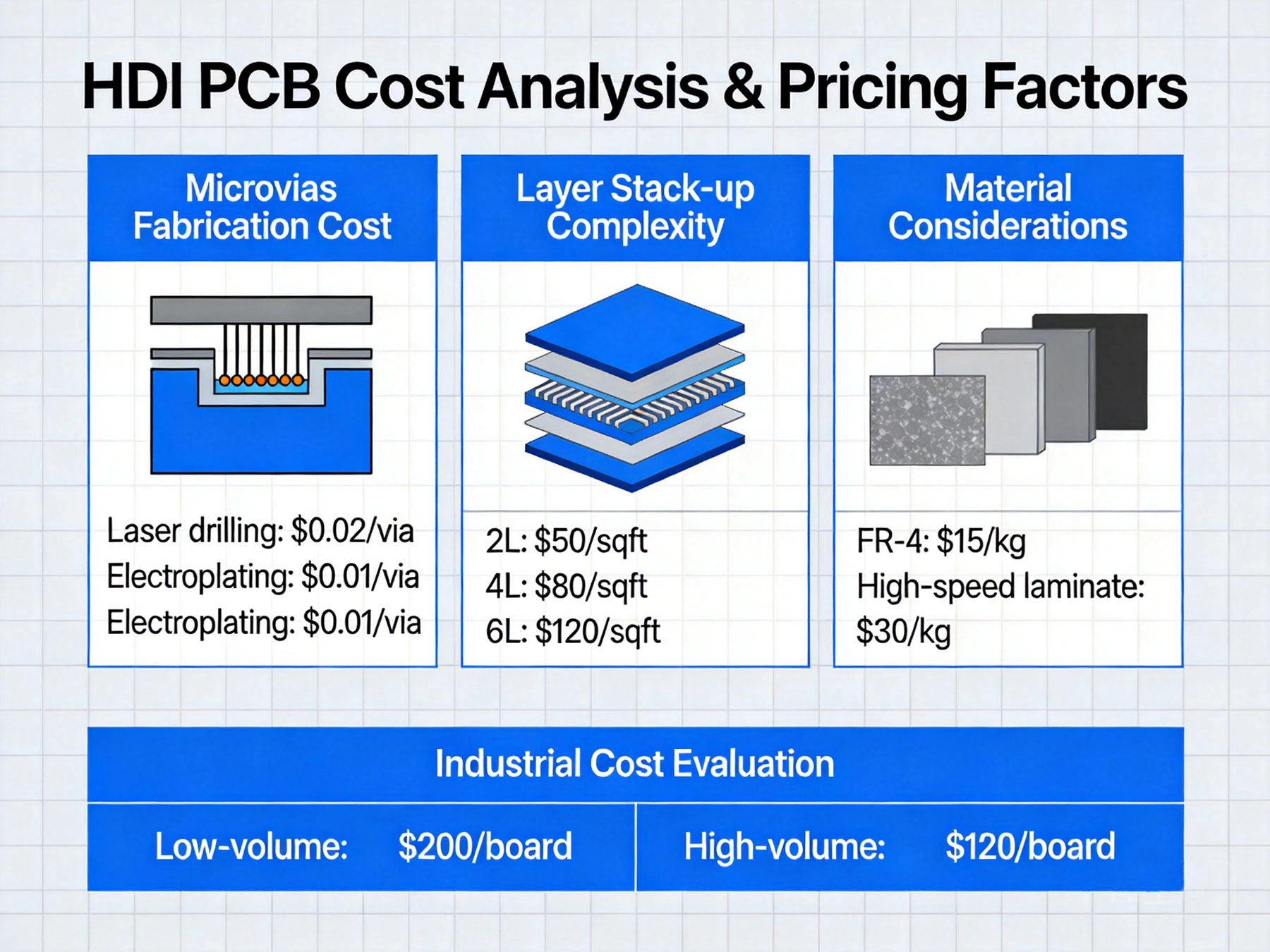
Laser Drilling is perhaps the single largest cost driver in Hdi Manufacturing:
A typical HDI board might have 100-1000 microvias. At 1-3 seconds per microvia, laser drilling time becomes significant. More microvias directly increase costs linearly with count.
Cost Optimization: Minimize microvia count. Use microvias only where truly needed rather than everywhere. Consider larger via structures where space allows.
Each build-up layer requires a complete lamination cycle:
A 2+N+2 HDI board with 4 build-up layers requires 4 lamination cycles compared to 1 cycle for conventional boards. Each lamination adds direct costs and opportunities for defects.
Cost Optimization: Use the minimum number of build-up layers required. Many designs work well with 1+N+1 when the designer assumes 2+N+2 is necessary.
Filling microvias with copper requires special plating:
Improper microvia plating causes reliability issues, so manufacturers invest heavily in process control and quality verification, adding cost.
Cost Optimization: Design microvias with appropriate aspect ratios (depth:diameter ratios under 0.8:1). Deeper microvias are more challenging to plate and more expensive.
HDI boards require more thorough electrical testing:
A 12-layer HDI board might have thousands of nets to test, requiring significant test time. Testing costs scale with complexity and layer count.
Cost Optimization: Provide clear test requirements. Specify what must be tested versus what can be sampled. Work with manufacturers to optimize test plans without compromising quality.
Layer count is one of the most significant cost drivers:
Typical cost increase per layer pair (adding 2 layers):
Cost increases are non-linear—the first layer additions (2 to 4, 4 to 6) have the biggest percentage impact.
Cost Optimization: Use the minimum layer count that provides adequate routing and power distribution. Many designs use more layers than necessary out of habit rather than requirement.
The number of microvias directly impacts cost:
Microvia density (microvias per square inch) also matters. Very dense microvia clusters create processing challenges that increase costs.
Cost Optimization: Minimize microvia count through careful routing. Use larger vias where space allows. Avoid unnecessary microvias—every microvia adds cost.
Fine lines and spaces increase costs:
Typical cost impact by line/space:
Pushing below standard capabilities always adds cost. Stay above manufacturer's minimum capabilities when possible.
Cost Optimization: Use the largest line and space dimensions your design tolerates. Many designers default to the minimum when larger dimensions would work fine.
Board size affects cost in several ways:
Panel utilization is critical. If your board size doesn't fit well on standard panel sizes, manufacturers may charge more due to material waste.
Cost Optimization: Design for standard panel sizes when possible. Work with manufacturers on panelization strategies to maximize utilization. Slightly adjusting board dimensions can dramatically improve efficiency.
Different surface finishes have different costs:
Cost difference between HASL and ENIG can be 20-30%. However, HDI boards typically require ENIG or similar finishes for fine-pitch components.
Cost Optimization: Choose the least expensive finish that meets your requirements. For many applications, OSP provides adequate performance at lower cost than ENIG.
Different core materials have different costs:
Standard FR-4 works for most industrial and consumer applications. Only specify premium materials when your application truly requires them.
Cost Optimization: Use standard materials whenever possible. High-Tg materials are often specified unnecessarily when standard FR-4 would work fine.
Thinner dielectrics enable more layers but increase costs:
Thin dielectrics are necessary for HDI but add handling complexity and lower yields. Use the minimum thickness that provides adequate performance.
Cost Optimization: Balance layer count with dielectric thickness. More layers with thicker materials may be less expensive than fewer layers with ultra-thin materials.
Copper thickness affects costs:
Thicker copper is needed for high current but increases processing costs. Specify copper weight based on actual current requirements, not habit.
Cost Optimization: Calculate actual current requirements rather than defaulting to heavier copper. Many designs use heavier copper than necessary out of caution.
Pricing changes at specific quantity thresholds:
Per-unit costs often drop 40-60% from prototype to production volumes. The exact break points vary by manufacturer.
Cost Optimization: Plan quantities to hit volume break points. Ordering slightly higher quantities can dramatically reduce per-unit cost.
Non-Recurring Engineering (NRE) charges cover setup costs:
NRE charges are one-time costs amortized over production quantity. For small quantities, NRE can exceed material costs. For large volumes, NRE becomes insignificant per unit.
Cost Optimization: For ongoing production, NRE is a one-time investment. For one-off prototypes, consider whether NRE charges are justified.
Committing to long-term production can reduce costs:
Manufacturers offer pricing incentives for predictable, long-term volume.
Cost Optimization: For ongoing products, negotiate long-term agreements with volume commitments.
Controlled impedance adds cost:
Single impedance requirements add 5-10% cost. Multiple impedance requirements add more.
Cost Optimization: Specify impedance requirements only where truly needed. Use standard impedance values where possible.
Blind and Buried Vias increase costs:
Any-layer Hdi with microvias on every layer maximizes flexibility but maximizes cost.
Cost Optimization: Use Blind Vias only on outer layers. Limit Buried Vias to truly necessary locations.
Special finishes increase costs:
Only specify special finishes when required by your application.
Cost Optimization: Evaluate whether special finishes are truly necessary or if alternatives exist.
Comprehensive testing adds cost:
More thorough testing directly increases costs. Balance testing thoroughness with cost.
Cost Optimization: Specify testing requirements precisely. Don't over-test beyond what your product truly needs.
Faster delivery increases costs:
Standard lead times (2-3 weeks) have no rush charges. Rush jobs (1 week or less) can add 30-50% to costs.
Cost Optimization: Plan ahead and avoid rush charges whenever possible. Build realistic schedules with buffer time.
Pricing fluctuates with demand:
Timing affects pricing. Launching during peak industry cycles may increase costs.
Cost Optimization: Schedule production when possible to avoid peak demand periods.
Lower yields effectively increase costs:
Complex HDI boards may have first-pass yields of 85-90% versus 95%+ for conventional boards. The difference represents real cost impact.
Cost Optimization: Design for manufacturability to improve yields. Simple designs with generous tolerances yield better and cost less.
HDI designs can affect assembly costs:
PCB costs don't exist in isolation—HDI PCBs often enable components that increase assembly costs.
Cost Optimization: Consider total product cost (PCB + assembly) when evaluating HDI economics.
Design changes create additional costs:
Each design iteration adds cost. Getting the design right the first time saves significant money.
Cost Optimization: Invest in thorough DFM review before prototyping. Catch issues in design rather than production.
Integrate cost considerations from the beginning:
The most cost-effective designs are those that meet requirements with minimum HDI complexity.
Challenge every design assumption:
Designers often include features out of habit rather than necessity. Questioning assumptions reveals cost-saving opportunities.
Choose manufacturers strategically:
The cheapest quote isn't always the best value. Consider total cost including quality, reliability, and support.
Plan quantities strategically:
Thoughtful quantity planning optimizes per-unit costs across the product lifecycle.
Provide complete information for accurate quotes:
Incomplete or inaccurate data leads to inaccurate quotes and later cost surprises.
Compare quotes carefully:
The lowest price quote may not represent the best value when you consider all factors.
Look for negotiation opportunities:
Manufacturers often offer pricing incentives for predictable, long-term volume relationships.
Hdi Pcb costs are higher than conventional boards for good reason—the technology enables capabilities that would be impossible otherwise. Understanding cost drivers helps you make informed decisions about when and how to use Hdi Technology most effectively.
The key isn't avoiding HDI costs entirely—it's using HDI where it provides genuine value while avoiding unnecessary complexity. Many designs include HDI features out of habit or misunderstanding rather than necessity. Careful design, thoughtful specification, and strategic manufacturer selection can significantly reduce costs without compromising performance.
When evaluating HDI costs, consider total product value: smaller enclosures, improved performance, and competitive advantages enabled by HDI capabilities often offset the higher PCB cost. The cheapest PCB option isn't always the best business decision.
Work with your manufacturer early in design to identify cost optimization opportunities. The best manufacturers provide DFM feedback that catches issues and suggests improvements before they become expensive problems in production.
By understanding cost drivers and making smart design trade-offs, you can achieve the benefits of HDI technology while controlling costs. HDI enables remarkable capabilities—use it strategically and optimize wisely to create cost-effective, high-performance products.
HDI PCBs typically cost 50-150% more than conventional PCBs depending on complexity. Simple 1+N+1 HDI might cost 1.5-2.0x conventional, while complex any-layer HDI can cost 2.5-3.5x. Actual costs vary based on board size, quantity, features, and manufacturer capabilities.
Laser drilling for microvias is typically the single largest cost driver. Laser drilling equipment is expensive, the process is slow, and each microvia requires drilling, plating, and testing time. Microvia count directly correlates with cost—the more microvias, the higher the cost.
Yes, layer count significantly affects cost. Each additional layer pair adds material costs, lamination cycles, and processing steps. Typical cost increases: 2→4 layers (+60-80%), 4→6 layers (+40-50%), 6→8 layers (+30-40%). The first layer additions have the biggest percentage impact.
Minimize microvia count by using them only where necessary, use the minimum layer count required, select the least expensive surface finish that meets requirements, use standard materials (FR-4) instead of premium materials unless necessary, and work with your manufacturer on DFM optimization during design rather than after.
Yes, quantity dramatically affects pricing. Prototype quantities (1-5 units) have the highest per-unit costs including full setup. Per-unit costs often drop 40-60% from prototype to production volumes (1,000+ units). Hitting volume break points can dramatically reduce per-unit costs.
Rush charges can add 20-50%+ to HDI PCB costs. Standard lead times (2-3 weeks) have no rush charges. Rush jobs (1 week or less) require expedited processing, off-cycle production, and often premium shipping, all adding significant cost. Plan ahead to avoid rush charges.
No, the lowest quote doesn't always represent the best value. Consider total cost including quality, reliability, delivery consistency, and technical support. The cheapest option often becomes most expensive in the long run due to quality problems, delays, and lack of support. Evaluate comprehensive value, not just price.
Include complete Gerber files (all layers, drill files, routing), detailed BOM with manufacturer part numbers, clear specifications (materials, finishes, tolerances), quantity requirements, timeline expectations, and any special testing or certification requirements. Complete information prevents pricing surprises later.
How to Read and Interpret HDI PCB Stack-up Drawings?July/14/2026
Troubleshooting Common Issues in HDI PCB AssemblySeptember/09/2026
Understanding HDI Terminology: A Glossary for EngineersAugust/03/2026
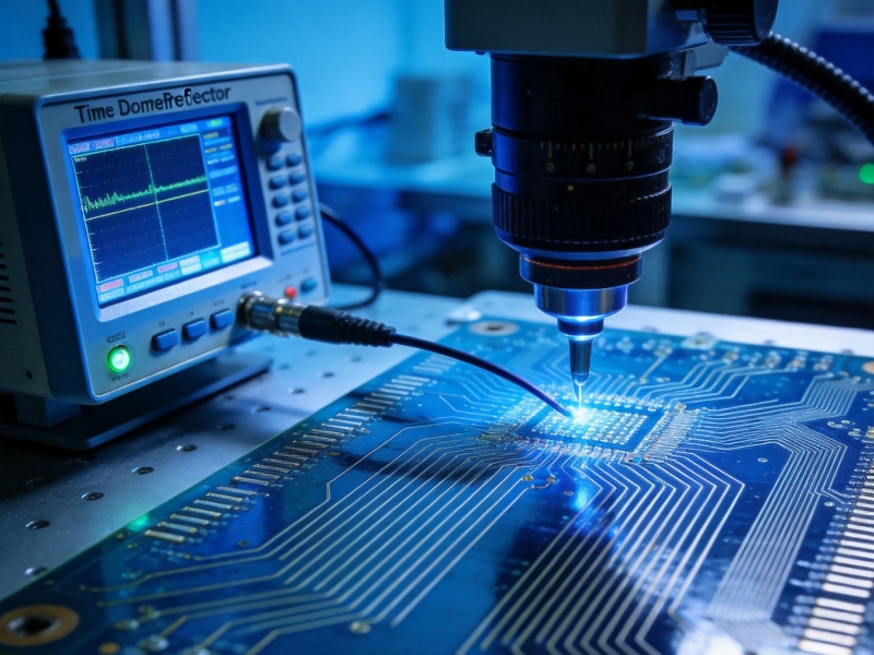
How to Measure and Control Impedance Tolerance in HDI BoardsAugust/03/2026
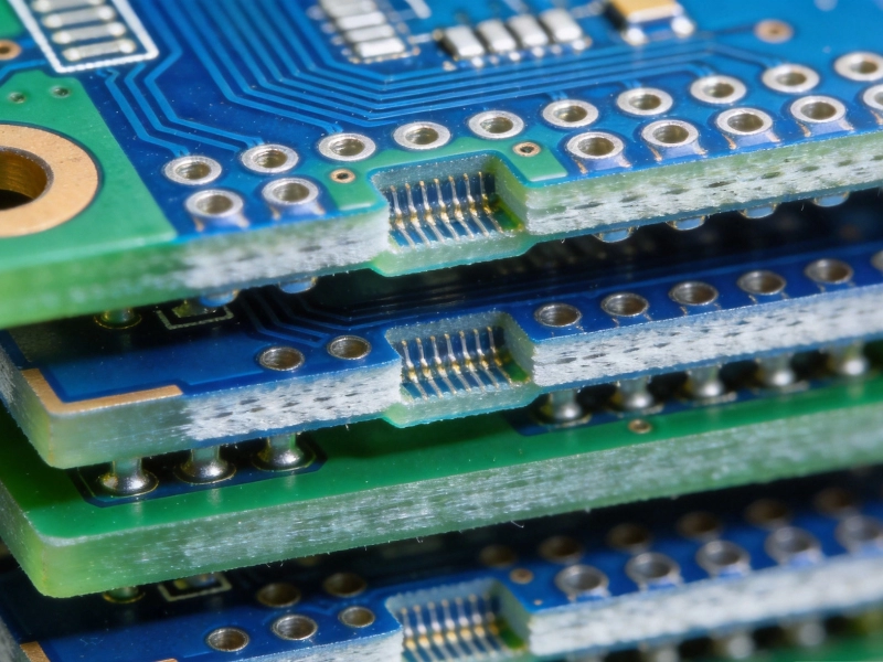
An Introduction to Microvia Technology in HDI PCBsJuly/24/2026
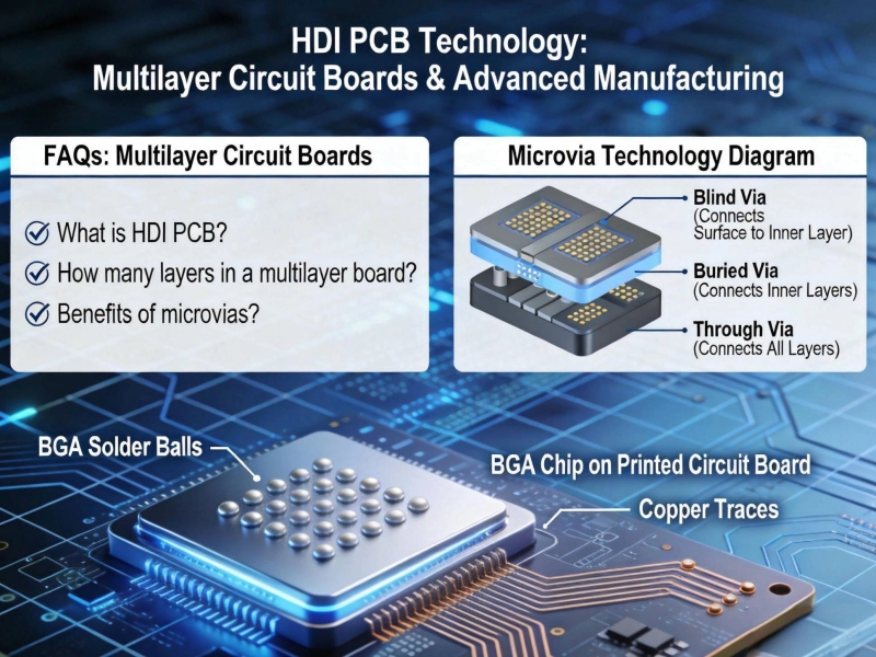
Top 10 Frequently Asked Questions About HDI PCB TechnologyMay/28/2026

Implementing a Robust Quality Control System for HDI ManufacturingJune/15/2026
Designing HDI Boards to Withstand Extreme Aerospace EnvironmentsJuly/22/2026