Open Nav

Hdi Pcb technology is one of the most transformative developments in electronics manufacturing of the past two decades. From smartphones and wearables to automotive Adas Systems and medical implants, HDI (High-density Interconnect) Pcb Technology enables the miniaturization, performance, and functionality that modern electronics demand. But with its specialized materials, manufacturing processes, and design requirements, HDI raises many questions for engineers, procurement professionals, and product managers who are new to the technology. This guide answers the top 10 most frequently asked questions about HDI PCBs, drawing on real questions from thousands of engineers and buyers who work with us every year.
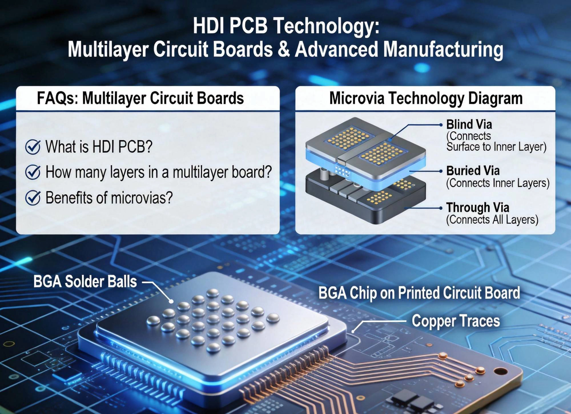
HDI stands for High-density Interconnect, and an Hdi Pcb is a printed circuit board that uses advanced manufacturing technologies to achieve significantly higher circuit density than conventional PCBs. The defining characteristics of HDI technology include:
The term "HDI PCB" encompasses a range of construction types, from simple 1+N+1 boards (with one buildup section) to complex any-layer constructions with 10+ buildup layers. The common thread is the use of Microvia Technology to achieve density that is not possible with conventional Pcb Manufacturing.
Hdi Pcb Technology delivers several compelling advantages that make it essential for modern electronics:
This is HDI's primary advantage. By using microvias and fine lines, HDI enables the same functionality in 40-60% less board area compared to standard multilayer construction. For smartphones, this is what makes it possible to pack powerful processors, multiple cameras, 5G radios, and large batteries into devices that fit in your pocket.
Shorter signal paths (due to any-layer interconnection), reduced via stub length, and thinner dielectrics all contribute to better electrical performance at high frequencies. HDI PCBs have lower capacitance between layers, faster signal propagation, and less signal loss at microwave and millimeter-wave frequencies. This is why HDI is the technology of choice for 5G, Wi-Fi 6/7, and high-speed digital applications.
Smaller boards with thinner dielectrics and fewer layers mean lighter products. For aerospace, automotive, and portable electronics, every gram matters. HDI enables weight savings of 30-50% compared to equivalent standard PCB implementations.
Any-layer HDI construction gives designers unprecedented flexibility to optimize routing, place components on any layer, and create efficient fan-out patterns for BGA packages. This flexibility accelerates new product development and enables designs that would simply be impossible with standard Pcb Technology.
While HDI's fine features may seem fragile, properly manufactured Hdi Boards can actually be more reliable than standard boards in many applications. The shorter thermal paths in microvias reduce thermal stress, and the absence of through-hole stubs eliminates a common failure mechanism. For applications with severe thermal environments, HDI with appropriate materials can outperform conventional boards.
A Microvia is a small via (plated-through electrical connection between PCB layers) with a diameter typically between 0.1mm and 0.3mm. This is the defining feature of HDI technology and the reason HDI PCBs can achieve dramatically higher density than conventional boards.
Unlike conventional through-hole vias which are drilled mechanically after all layers are stacked, microvias are formed before or during the buildup process. The most common methods:
The diameter of a via determines how many vias can fit in a given area, which directly limits routing density. A 0.3mm diameter via occupies roughly 9x more board area than a 0.1mm diameter via. For complex chips with thousands of connections (high-pin-count BGAs), the ability to route traces between the vias — not just fit the vias — requires the smallest possible via diameters.
Understanding the differences between HDI and standard multilayer PCBs helps you choose the right technology for your application:
| Feature | Standard Multilayer Pcb | HDI PCB |
|---|---|---|
| Via Technology | Mechanically drilled through-hole vias (0.3mm+ diameter) | Laser-drilled microvias (0.1-0.3mm diameter) |
| Trace Width/Spacing | 100-150 microns typical | 50-75 microns typical |
| Dielectric Thickness | 100-200 microns | 50-100 microns |
| Layer Interconnection | Through-hole vias connect all layers | Blind/buried microvias connect specific layers |
| Typical Layer Count | 2-8 layers | 4-20+ layers |
| Routing Density | Moderate | High to Very High |
| Manufacturing Process | Standard lamination, mechanical drill | Sequential Lamination, laser drill, buildup |
| Minimum Feature Size | ~150 microns | ~50 microns |
| Typical Cost Premium | Baseline | 20-100% above standard |
| Primary Applications | Consumer electronics, simple products | Smartphones, advanced computing, automotive |
The key architectural difference is that standard multilayer PCBs use through-hole vias that connect every layer from top to bottom, while HDI uses blind and buried microvias that connect only specific layers. This "any-layer" interconnection capability is what gives HDI its flexibility and density advantage.
HDI PCB construction comes in several variants, each with different complexity, density capability, and cost:
The simplest HDI configuration: one buildup layer on one side of a core. This adds moderate density improvement while keeping manufacturing simple. Common in smartphones for the chip-on-board region while the rest of the board uses standard construction.
A conventional core with buildup layers on one or both sides. The core is built first using standard processes, then HDI buildup layers are added on top. This is the most common HDI configuration, balancing density improvement with manufacturing practicality.
Two buildup sections on each side of the core, enabling higher density and more routing flexibility. This is common in smartphones and other high-density consumer products.
The highest-complexity HDI construction, where microvias can connect any two adjacent layers. This eliminates the fixed layer assignments of traditional multilayer design and provides maximum routing flexibility. Any-layer HDI is what enables the ultra-thin, multi-chip smartphone modules found in flagship phones.
HDI construction with embedded passive components (resistors, capacitors) buried within the PCB layers. This further reduces board area by eliminating discrete passive components from the surface. Growing in adoption for space-constrained applications.
HDI PCB applications span across every industry where miniaturization, performance, and reliability converge:
Smartphones are the largest single application for HDI PCBs. A modern smartphone contains 6-12 HDI boards: the main processor board, display modules, camera modules, RF boards, and more. All use HDI to pack maximum functionality into minimum space. Wearables (smartwatches, fitness trackers), tablets, laptops, and gaming devices similarly depend on HDI technology.
Automotive ADAS (Advanced Driver Assistance Systems), infotainment systems, instrument clusters, and engine control units increasingly use HDI PCBs. Automotive HDI must meet stringent reliability standards (AEC-Q100, IATF 16949) and operate across extreme temperature ranges (-40°C to +125°C). The trend toward autonomous driving is accelerating HDI adoption in automotive.
Implantable medical devices (pacemakers, cochlear implants, neurostimulators), diagnostic equipment, and portable medical devices use HDI for miniaturization and reliability. Medical HDI applications often require the highest reliability grades and FDA compliance documentation.
Data center switch boards, router line cards, GPU modules, and AI accelerator boards use HDI to accommodate high-pin-count ASICs, maintain Signal Integrity at 25-100+ Gbps data rates, and manage thermal density. The explosion of AI workloads is driving rapid growth in HDI for data center applications.
IoT devices — from smart home sensors to industrial monitoring systems — use HDI PCBs for the combination of small size, wireless connectivity (Wi-Fi, BLE, Zigbee), and low power consumption. Many IoT modules use chip-on-board HDI construction to minimize size and cost.
Radar systems, satellite electronics, avionics displays, and communication systems use HDI for the combination of high reliability, miniaturization, and the ability to handle complex signal routing at high frequencies. These applications require the most rigorous qualification and testing programs.
Hdi Pcb Cost is typically 20-100% higher than equivalent standard multilayer PCBs, depending on the HDI construction complexity. Understanding the cost drivers helps you make informed decisions:
| HDI Type | Cost Premium vs Standard | When It Makes Sense |
|---|---|---|
| 1+0+1 (Single buildup) | 20-40% higher | Moderate density needs, cost-sensitive applications |
| 1+N+1 (Core-buildup) | 40-60% higher | Most common choice, balanced cost and density |
| 2+N+2 (Dual-buildup) | 60-80% higher | High density, space-constrained designs |
| Any-Layer HDI | 80-100%+ higher | Extreme miniaturization, flagship devices |
The higher cost of HDI is justified when the benefits outweigh the cost premium:
Hdi Pcb Design presents unique challenges that differ from standard PCB design:
HDI design rules are more complex than standard PCB rules. Designers must manage:
Many HDI designs require multiple design-for-manufacturing (DFM) iterations before the design is producible. Designers who are new to HDI often specify features that cannot be reliably manufactured at volume. Budget time and budget boards for DFM feedback cycles, especially on first HDI designs.
While HDI provides better Signal Integrity for high-speed signals in principle, realizing this potential requires careful attention to:
High component density concentrates heat generation. Thermal design for HDI requires:
Hdi Manufacturing requires more detailed fabrication data than standard boards. Designers must provide:
Selecting the right HDI PCB manufacturer is one of the most important decisions in your product development process. Not all manufacturers can produce HDI reliably, and the difference between a capable HDI supplier and an incapable one can determine whether your product succeeds or fails.
Hdi Pcb Technology continues to evolve as electronics demand greater miniaturization, performance, and functionality. Here are the major trends shaping the future of HDI:
The industry is pushing toward trace widths below 50 microns (2 mil) using advanced lithography and modified semi-additive process (mSAP) techniques. This enables even higher routing density and is being driven by the latest generation of 5nm and 3nm semiconductor packages that require ultra-fine fan-out routing.
Embedding passive components (resistors, capacitors) and active components (ICs) within PCB layers is moving from research to production. This eliminates components from the surface, reducing board size and improving electrical performance by shortening signal paths. Emerging embedded component technologies include:
Automotive Electronics, AI accelerators, and networking switches are driving demand for HDI boards with 20, 30, and even 40+ layers. These ultra-complex boards require advanced manufacturing capabilities and sophisticated quality systems to produce reliably at volume.
The rollout of 5G sub-6GHz and millimeter-wave (mmWave) networks is driving demand for HDI substrates with controlled dielectric constant (Dk) and low loss tangent (Df). Advanced materials including hydrocarbon ceramic, PTFE composites, and special resin systems are being developed to meet the demanding electrical and thermal requirements of 5G infrastructure and devices.
Environmental regulations are driving changes in Pcb Materials and processes. Halogen-free substrates, lead-free finishes, and RoHS/REACH compliance are now standard requirements. The industry is also exploring bio-based substrate materials and more efficient manufacturing processes that reduce material waste and energy consumption.
The semiconductor industry's shift from monolithic chips to chiplet architectures is creating new opportunities for HDI technology. High-density interconnect substrates that connect multiple chiplets — including interposers, fan-out substrates, and HDI build-up on glass — represent the next frontier in HDI development.
Hdi Manufacturing is becoming more digital and data-driven. Real-time process monitoring, AI-based defect detection, digital twin simulation, and automated DFM feedback are making HDI manufacturing more consistent and yield-predictable. These technologies are reducing the expertise barrier that has traditionally made HDI design challenging.
Our engineering team has extensive experience supporting HDI PCB projects from concept through production. We provide design for manufacturing review, material selection consultation, prototyping, and full-scale production with comprehensive quality assurance. Contact us to discuss your HDI requirements and see how we can help bring your product to market faster.

Implementing a Robust Quality Control System for HDI ManufacturingJune/15/2026
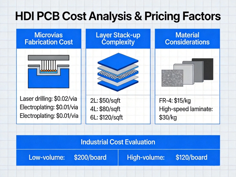
HDI PCB Cost Guide: What Factors Drive the Price Up?June/16/2026
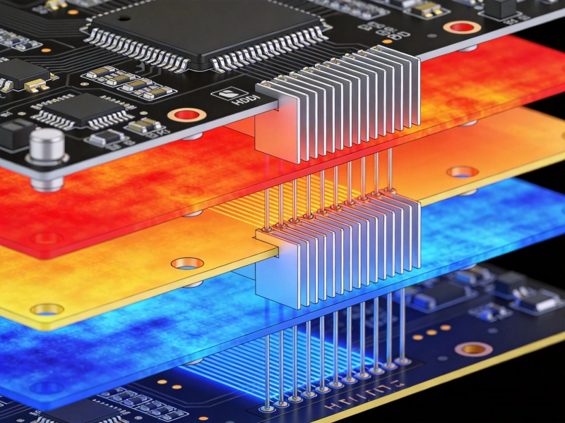
Effective Thermal Management Strategies for High-Density PCBsMay/28/2026
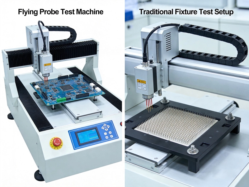
Flying Probe vs. Fixture Testing: Which is Best for HDI PCBs?June/11/2026
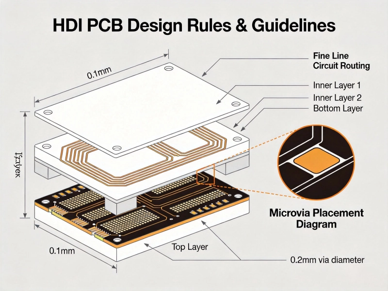
Essential HDI PCB Design Rules for Beginners and ExpertsMay/28/2026
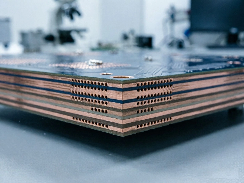
Understanding Sequential Lamination in Multi-Step HDI BoardsJuly/03/2026
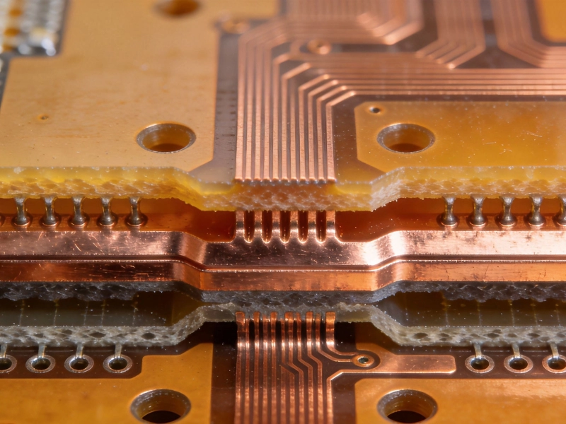
FR-4 vs. High-Tg Materials: What Works Best for HDI Applications?July/07/2026
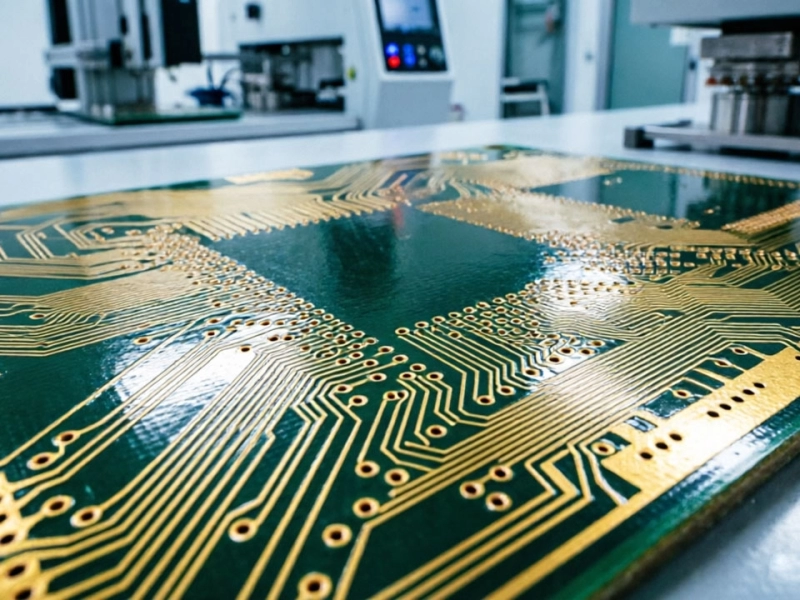
Selecting the Right Dielectric Materials for High-Performance HDI PCBsJune/05/2026