Open Nav

As electronic devices continue shrinking in size while expanding in functionality, the demands placed on printed circuit board technology have grown exponentially. Smartphones now pack more processing power than desktop computers did a decade ago, while AI servers require interconnects that push the boundaries of what traditional Pcb Manufacturing can achieve. At the heart of this technological advancement lies Sequential Lamination—a sophisticated manufacturing approach that enables the creation of High-density Interconnect boards capable of supporting the complex routing, Miniaturization, and performance requirements of modern electronics.
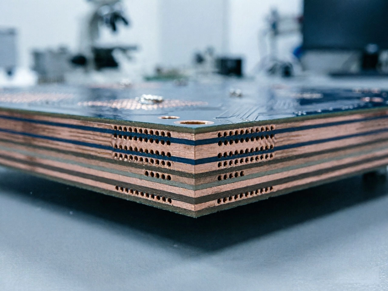
Sequential Lamination represents a multi-step build-up manufacturing process where PCB layers are constructed incrementally rather than being pressed together in a single operation. Unlike traditional multi-layer board fabrication, which laminates all layers simultaneously under high temperature and pressure, sequential lamination adds one or more layers at a time through repeated cycles of dielectric application, pattern deposition, and compression bonding. This incremental approach enables the creation of complex layer structures incorporating Blind Vias, Buried Vias, and Microvias that would be impossible to achieve through conventional manufacturing methods.
The fundamental advantage of sequential lamination lies in its ability to create electrical connections between non-adjacent layers without consuming routing space on intermediate layers. Blind Vias connect surface layers to inner layers without penetrating through the entire board thickness, while Buried Vias connect inner layers that remain hidden from both surfaces. These specialized via structures enable dramatic increases in routing density, allowing more signal traces to occupy the same board area while maintaining the Signal Integrity that modern high-speed circuits demand.
Traditional Pcb Manufacturing evolved around through-hole technology where all layers are fabricated individually and then laminated together in a single pressing operation. This approach works well for relatively simple multi-layer boards but reaches fundamental limitations when attempting to create the ultra-high densities required for modern applications. The through-hole via, which must pass through the entire board stack, consumes routing space on every intermediate layer and creates stubs that degrade signal quality at high frequencies.
Sequential lamination emerged as a solution to these limitations, initially in military and aerospace applications where cost was secondary to performance. The technology has since proliferated into consumer electronics, telecommunications infrastructure, and high-performance computing, driven by consumer demand for smaller devices and industrial requirements for greater computing density. Today, the AI server market has pushed Hdi Technology to extreme levels, with boards requiring 5-6 stages of sequential lamination or even Any-layer Hdi configurations reaching 70-78 total layers.
The HDI build-up process centers on the systematic addition of dielectric and conductive layers using controlled materials and precision equipment. Each build-up stage creates new routing layers, forms inter-layer connections through Microvia Technology, and builds the foundation for subsequent layers. This incremental approach provides manufacturing flexibility that single-press lamination cannot match, enabling complex stack-ups with specific routing characteristics optimized for particular signal types or power distribution requirements.
Dielectric Material selection critically impacts sequential lamination success and final board performance. Prepreg materials—fiberglass fabric impregnated with partially cured resin—serve as the primary dielectric medium in sequential build-up. The resin content, glass transition temperature (Tg), and flow characteristics of prepreg must match the specific requirements of each build-up stage, accounting for the filling of existing topography, bond strength requirements, and subsequent processing temperatures.
Advanced Hdi Manufacturing increasingly employs resin-coated copper (RCC) and liquid dielectric materials for finer feature control. These materials enable tighter registration tolerances and more uniform dielectric thickness than traditional prepreg, supporting the Microvia densities and fine-line routing that distinguish state-of-the-art Hdi Boards. Material compatibility across sequential layers requires careful engineering to ensure that subsequent processing does not degrade previously formed structures.
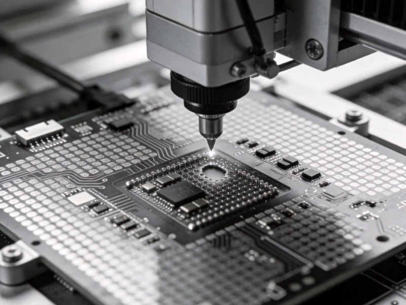
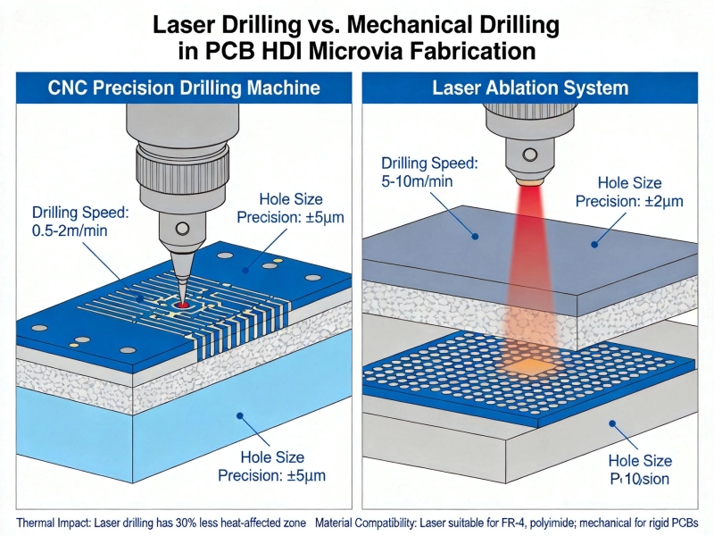
Laser Drilling has replaced mechanical drilling for Microvia formation in Hdi Boards, enabling via diameters below 100 micrometers with positional accuracy of ±5 micrometers. Carbon dioxide (CO2) lasers create vias in organic dielectrics through thermal ablation, while ultraviolet (UV) lasers provide superior control for sensitive applications. The Laser Drilling process creates clean, consistent microvia walls without the smear and burring associated with mechanical drilling, enabling reliable electrical connections at the densities Hdi Applications demand.
Microvia Design in sequential lamination must account for the specific build-up sequence and subsequent processing exposures. Via aspect ratio—the ratio of depth to diameter—determines whether vias can be reliably plated and filled. Stacked Microvias, where vias in successive layers align vertically, maximize routing density but require precise depth control and excellent registration across lamination cycles. Staggered microvias, where adjacent layer vias offset horizontally, provide better manufacturing margin while still achieving significant density improvements over through-hole technology.
The sequential lamination process follows a defined sequence of manufacturing steps that repeat across multiple build-up stages. Understanding this process flow reveals how individual manufacturing operations combine to create complex HDI structures impossible to achieve through simpler methods.
Sequential lamination typically begins with a multi-layer core substrate manufactured through traditional methods. This core provides the mechanical foundation and initial routing layers from which the HDI build-up extends. Core construction follows standard multi-layer processes including inner layer patterning, oxide treatment, lay-up, and pressing. The finished core undergoes electrical testing to verify inner layer connectivity before committing to the expensive sequential build-up process.
The first HDI build-up stage begins with surface preparation of the core, ensuring proper adhesion for subsequent dielectric application. Dielectric Material—prepreg, RCC, or liquid dielectric—is applied across the core surface, filling any topography created by existing circuitry. The dielectric is partially or fully cured, creating a smooth insulating surface from which subsequent routing layers will be formed. Laser drilling then creates microvia openings to underlying layers, followed by desmear and activation processes that prepare via walls for metallization.
Via metallization deposits conductive material on dielectric surfaces and inside microvia openings, creating electrical connections to underlying layers. Electroless Copper Plating initiates the metallization process, depositing a thin copper seed layer across all exposed surfaces including via sidewalls. Electrolytic Copper Plating then builds the conductive layer to the thickness required for current-carrying capacity and manufacturing robustness. The combined metallization process must achieve void-free copper inside microvias to ensure reliable long-term electrical connections.
Patterning defines the circuit traces that comprise each routing layer through photolithographic processes. Dry film or liquid photoimageable resist is applied over the copper surface, exposed to UV light through a photomask containing the circuit pattern, and developed to reveal copper where traces will remain. Copper not protected by resist is removed through chemical etching, leaving the patterned circuit traces that form the new routing layer. Surface planarization, when required, ensures that subsequent build-up stages proceed from a flat substrate.
Each subsequent build-up cycle repeats the dielectric application, microvia formation, metallization, and patterning sequence to add additional routing layers. The number of build-up stages determines the HDI stage designation: a 1+N+1 board has HDI layers on both surfaces of a traditional core, while a 4+N+4 board adds four build-up layers to each side. Higher stage counts enable greater routing density but impose compounding registration challenges and longer manufacturing cycle times.
Registration accuracy becomes increasingly critical with each successive build-up stage. Each lamination cycle introduces slight dimensional changes as materials flow and cure under pressure and temperature. Accumulated registration errors from multiple build-up stages can exceed tolerance limits for fine-pitch components, requiring sophisticated compensation strategies in design and manufacturing. Leading HDI manufacturers employ advanced imaging systems, statistical process control, and optimized lamination parameters to maintain registration within required tolerances across complex multi-stage builds.
HDI board Stack-up Design determines the routing capacity, Signal Integrity performance, and manufacturing complexity of the final product. Understanding common stack-up configurations helps designers select appropriate structures for specific application requirements.
The simplest HDI configurations add a single build-up layer to each side of a traditional core (1+N+1) or two layers to each side (2+N+2). These configurations provide meaningful density improvements over through-hole technology while maintaining relatively straightforward manufacturing requirements. The 1+N+1 structure is particularly common in consumer electronics applications such as smartphones and tablets, where moderate density improvements suffice for the form factor constraints involved.
2+N+2 configurations offer higher routing density suitable for more complex applications. The additional build-up layers enable finer escape routing from high-density component packages such as area array components with hundreds of pins. Manufacturing complexity increases with additional build-up stages, but the fundamental processes remain well within the capabilities of experienced HDI manufacturers. Many smartphone motherboards employ 2+N+2 or similar configurations to achieve the routing density required for sophisticated mobile processors and memory packages.
Any-layer Hdi represents the pinnacle of sequential lamination technology, where every layer in the board stack is built sequentially with microvia connections between any adjacent pair of layers. This configuration eliminates the distinction between core layers and build-up layers, enabling routing traces on any layer to connect to any other layer through microvia chains. Any-layer HDI achieves the ultimate in routing flexibility and density, enabling designs with extremely high connection counts in minimal board areas.
The manufacturing complexity of any-layer HDI substantially exceeds simpler configurations. Six or more sequential lamination stages may be required for typical any-layer boards, with each stage demanding precise process control and comprehensive inspection. Manufacturing yields for any-layer HDI run lower than for simpler configurations, contributing to higher per-board costs. These costs are justified in applications where board area constraints or performance requirements demand any-layer capabilities—high-end smartphones, advanced graphics processors, and telecommunications infrastructure where density and performance justify the investment.
Sequential lamination presents manufacturing challenges that require sophisticated process control, advanced equipment, and extensive expertise. Understanding these challenges illuminates why Hdi Manufacturing requires specialized facilities and why yield losses can significantly impact product costs.
Layer-to-Layer Registration represents the most demanding challenge in multi-step sequential lamination. Each build-up stage must align new features to underlying layers within tolerances often tighter than ±50 micrometers for fine-pitch components. The accumulated effects of material shrinkage, thermal expansion during lamination, and handling-induced distortion can exceed tolerance budgets if not properly managed through design compensation, process optimization, and statistical process control.
Manufacturers employ various strategies to maintain registration accuracy across sequential build-up stages. These include controlled-humidity storage to minimize moisture-induced dimensional changes, precision imaging systems with sub-micrometer resolution, optimized lamination parameters that minimize material flow and distortion, and statistical process monitoring that detects trends before they cause tolerance exceedances. The investment in registration capability represents a significant portion of HDI manufacturing equipment cost and process development effort.
Microvia Filling achieves void-free copper inside laser-drilled vias, ensuring reliable electrical connections that maintain integrity throughout product lifetime. Voids—trapped gas pockets within the plated copper—create reliability risks that may not surface until after assembly and field deployment. Void formation results from improper plating chemistry, inadequate desmear processing, or plating parameter issues that prevent complete copper deposition in via cavities.
Process control for Microvia Filling requires careful management of electroless copper activation, electrolytic copper plating solution composition, and current density parameters throughout plating cycles. Automated plating equipment with closed-loop process control maintains solution chemistry within tight limits, while statistical process monitoring detects deviations before they cause quality problems. Final inspection using cross-section analysis or X-ray imaging verifies microvia quality for critical applications.
Each sequential lamination stage subjects previously formed layers to additional thermal and mechanical processing. Materials must maintain structural integrity and electrical performance through multiple high-temperature exposures without degradation. The glass transition temperature (Tg) and decomposition temperature (Td) of dielectric materials must exceed the maximum temperatures encountered during subsequent processing, or else previously formed layers may soften, distort, or delaminate.
Copper-to-copper bonding between layers must achieve adequate peel strength to prevent delamination under thermal cycling or mechanical stress. Surface preparation before each lamination stage—whether oxide treatment, micro-etching, or plasma treatment—must create surfaces that bond effectively without damaging underlying circuitry. The interaction between surface preparation chemistry and dielectric material properties requires careful characterization and control to achieve consistent bonding across production lots.
Successful HDI design requires understanding how sequential lamination capabilities and constraints influence design decisions. Designers who understand manufacturing realities create more producible designs that achieve higher yields and lower costs than those who treat HDI as a simple technology extension.
Via-in-pad design, where microvias are placed directly in component pads rather than offset routing paths, maximizes routing efficiency by eliminating the space traditionally required for fan-out routing from component pins. This technique is essential for high-density area array packages where pin counts exceed what traditional fan-out can accommodate. Via-in-pad requires specialized manufacturing processes including via plugging or filling to create flat pad surfaces suitable for component attachment.
Stacked via configurations, where microvias in successive layers align vertically, enable the highest routing densities but require exceptional registration and depth control across multiple lamination cycles. The cumulative registration tolerance budget must accommodate the potential for misalignment between any pair of stacked via layers, limiting the practical number of stacked via layers. Design guidelines typically restrict stacked via configurations to two or three consecutive layers, with staggered via configurations providing better manufacturing margin for higher density requirements.
HDI structures present both opportunities and challenges for signal integrity. The short via lengths of microvias compared to through-holes reduce stub effects that degrade signal quality at high frequencies. Reduced via pad dimensions minimize capacitive loading that limits signal rise times. These characteristics make HDI attractive for high-speed digital applications including 224G SerDes links in AI servers and high-frequency RF circuits in communications systems.
However, the high density of HDI routing creates new signal integrity challenges. Reduced trace spacing increases coupling between adjacent signals, potentially causing crosstalk that degrades signal quality. The complex layer structures of sequential lamination require careful attention to reference plane continuity and power distribution network design. Designers must balance routing density against signal integrity requirements, often reserving outer routing layers for critical signals while using inner layers for less sensitive routing.
High-density HDI boards dissipate heat differently than traditional multi-layer boards, requiring Thermal Management strategies appropriate to the specific technology. The thin dielectrics and fine traces of HDI routing may limit heat spreading compared to traditional boards with thicker copper and larger thermal mass. Thermal relief structures, Thermal Vias, and embedded heat spreaders help manage heat in dense HDI assemblies.
Component attachment in HDI boards requires attention to thermal interface materials and attachment processes compatible with the fine-pitch components and high-density routing involved. Void formation during component attachment soldering can create hot spots that affect long-term reliability. Lead-free soldering processes, now mandatory in most applications, impose higher peak temperatures that stress HDI materials more severely than traditional tin-lead processes.
Quality assurance for sequential lamination requires comprehensive inspection and testing strategies that verify manufacturing success at each stage and detect defects before they propagate to expensive subsequent processing. The cumulative nature of sequential build-up means that early-stage defects may not become apparent until multiple subsequent stages complete, dramatically increasing the cost impact of quality escapes.
In-process inspection verifies manufacturing quality at each build-up stage before subsequent layers obscure underlying features. Automated Optical Inspection (AOI) examines circuit patterns for opens, shorts, and dimensional compliance. Automated X-ray Inspection (Axi) examines microvia quality and detects voids or misregistrations that would be invisible to optical inspection. These inspection processes add cycle time and cost but prevent defective boards from consuming additional manufacturing resources.
Electrical testing at intermediate build-up stages verifies layer connectivity before subsequent processing adds value. Netlist verification comparing actual electrical connectivity against design specifications catches errors including missing connections, unintended shorts, and incorrect via formation. This early electrical verification prevents costly scrap of multi-stage builds where defects would otherwise remain undetected until final testing.
Final testing for HDI boards encompasses both electrical verification and mechanical integrity assessment. Flying probe testing or fixture-based testing verifies complete netlist compliance for the finished assembly. High-potential (hipot) testing verifies dielectric integrity and insulation resistance. Thermal cycling or thermal shock testing assesses reliability under the temperature extremes that may be encountered in field service.
X-ray Inspection provides final verification of internal structures including microvia fill quality and buried feature geometry. Cross-section analysis, while destructive and applicable only to coupon samples, provides the most detailed verification of internal structure quality. These comprehensive testing approaches ensure that HDI boards meeting quality specifications provide the reliability required for demanding applications.
The demand for sequential lamination and Hdi Technology follows application requirements for Miniaturization, performance, and functionality that cannot be achieved through Traditional Pcb manufacturing approaches.
Smartphone evolution has driven HDI technology from specialized aerospace application to mainstream consumer Electronics Manufacturing. Modern smartphones contain any-layer HDI boards with six or more build-up stages, achieving routing densities that would be impossible through traditional through-hole technology. The form factor constraints of mobile devices—requiring complex circuitry in minimal volume—make HDI essential rather than optional.
Component miniaturization in mobile devices continues pushing HDI requirements. Each generation of mobile processors incorporates higher pin counts in smaller packages, requiring finer routing and more sophisticated escape patterns. Camera modules, display drivers, and power management circuits add additional complexity. The intense competition in mobile devices drives HDI manufacturers to continuously improve yields and reduce costs while maintaining the quality levels these demanding applications require.
AI servers represent the current frontier of Pcb Technology, with requirements that push beyond even the most sophisticated smartphone applications. The transition from 112G to 224G SerDes signaling in AI interconnects demands Pcb Materials and manufacturing precision that challenge conventional approaches. Backplanes and universal base boards (UBB) in AI servers may reach 70-78 layers with 5-6 stages of sequential lamination or any-layer HDI configurations.
The signal integrity requirements of high-speed AI interconnects demand controlled impedance, minimal loss, and precise registration across dozens of layers. Sequential lamination enables routing optimization that reduces stub effects and improves signal quality at frequencies where traditional through-hole vias would severely degrade performance. The investment in advanced HDI capability for AI servers is justified by the premium pricing and strategic importance of AI computing infrastructure.
Automotive Electronics are increasingly adopting HDI technology as vehicles incorporate more sophisticated electronics for driver assistance, infotainment, and electric powertrain control. Automotive reliability requirements—extended temperature ranges, Vibration Resistance, and multi-decade service life—demand manufacturing precision and material quality that sequential lamination can provide. The automotive industry's transition toward electric vehicles accelerates HDI adoption for Power Electronics and high-speed vehicle networking.
Automotive Quality management systems including Iatf 16949 impose stringent requirements on HDI manufacturing processes. Zero-defect quality goals require process capability indices (Cpk) that exceed typical manufacturing tolerances. The combination of demanding performance requirements and rigorous quality expectations positions advanced HDI manufacturing as essential capability for Automotive Electronics suppliers.
Sequential lamination has evolved from specialized aerospace technology to essential manufacturing capability for the electronic devices that define modern life. The incremental build-up approach that sequential lamination provides enables routing densities, signal integrity, and miniaturization that traditional manufacturing cannot achieve. Understanding this technology is essential for engineers and designers who create the next generation of electronic products.
The challenges of sequential lamination—registration accuracy, void-free microvia filling, material compatibility, and process control—represent engineering achievements in their own right. Manufacturers who master these challenges provide competitive advantage to the product teams who rely on HDI capability. As electronic applications continue demanding greater density and performance, sequential lamination technology will continue advancing to meet these requirements.
For design teams, understanding sequential lamination capabilities and constraints enables creation of more producible designs that achieve higher yields and lower costs. Collaboration with HDI manufacturing partners early in design development ensures that designs leverage available manufacturing capabilities without exceeding practical limits. This partnership approach—combining design expertise with manufacturing excellence—produces the innovative electronic products that continue transforming how we live and work.
Sequential lamination is the manufacturing process used to create HDI (High-density Interconnect) boards. HDI describes the end product—a board with higher routing density achieved through Microvia Technology—while sequential lamination describes how that product is manufactured through incremental layer-by-layer build-up. All HDI boards require sequential lamination, but not all sequential lamination produces HDI-density routing.
Current manufacturing technology supports six or more sequential build-up stages on each side of a board, enabling any-layer HDI configurations with routing on every layer. AI server applications may employ 5-6 build-up stages reaching total stack-ups of 70-78 layers. Practical limits depend on manufacturing capability, yield requirements, and cost constraints for specific applications.
Modern HDI manufacturing routinely produces microvias with diameters below 100 micrometers, with some processes achieving 50-75 micrometer diameters. Laser drilling technology with positioning accuracy of ±5 micrometers enables these fine features. Smaller microvia dimensions become increasingly difficult to plate reliably, creating practical limits on feature miniaturization.
Sequential lamination costs more due to multiple factors: additional manufacturing cycles requiring repeated equipment setup and processing; sophisticated laser drilling and advanced metallization processes; lower yields due to more complex manufacturing with more potential failure points; and extensive inspection and testing at each build-up stage. These costs are justified when applications require the routing density, signal integrity, or miniaturization that sequential lamination provides.
Blind vias connect surface layers to inner layers without penetrating through the entire board thickness. Buried vias connect inner layers that are not visible from either board surface. Sequential lamination creates these via types by forming connections during specific build-up stages rather than drilling through the completed board. These specialized vias enable routing densities impossible with traditional through-hole technology.
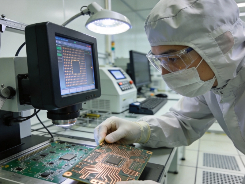
The Challenge of Plating and Filling Microvias in HDI ProductionJuly/26/2026
What is the Lead Time for Manufacturing Custom HDI Boards?October/12/2026
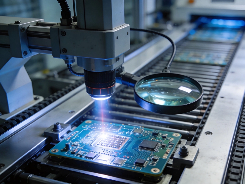
Critical Quality Checkpoints in the HDI Production LineJuly/13/2026
Overcoming Common Manufacturing Defects in High-Density InterconnectsSeptember/21/2026
How Manufacturers Achieve High Precision Alignment in 10+ Layer HDI BoardsAugust/15/2026
Precision in HDI FabricationJune/04/2026
Understanding the Role of Copper Foil Roughness in Signal IntegritySeptember/23/2026
The Role of HDI PCBs in Miniaturized Implantable Medical DevicesJuly/21/2026