
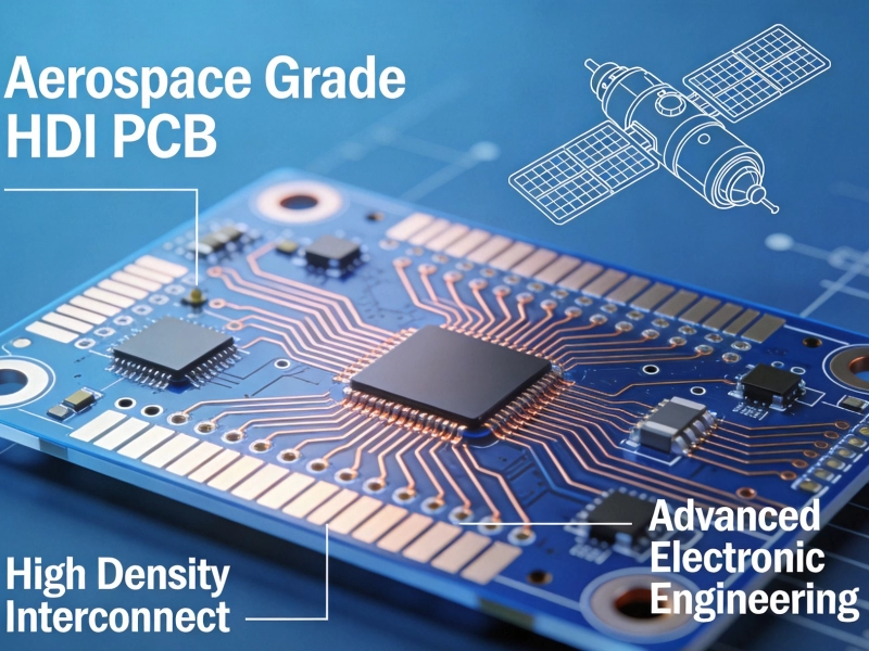
High-density Interconnect printed circuit boards have revolutionized aerospace Electronics Design. Mission-critical applications from satellite systems to flight control computers demand exceptional reliability, Miniaturization, and performance. Hdi Technology meets these requirements through advanced via structures, fine-line routing, and multilayer construction. This comprehensive guide examines the unique requirements governing Hdi Pcb deployment in aerospace environments.

Aerospace applications impose extreme environmental stresses on electronic components. Unlike consumer electronics operating in climate-controlled environments, aerospace PCBs encounter temperature swings from -55°C to +125°C during operation. Satellites experience rapid thermal cycling as they transition between Earth's shadow and direct sunlight. Launch vehicles endure intense vibration and mechanical shock during ascent.
Radiation presents another critical challenge. Orbiting satellites encounter ionizing radiation from solar particles and cosmic rays. This radiation causes cumulative damage to semiconductor devices and can trigger single-event upsets in digital circuits. PCBs must incorporate radiation-hardened components and maintain Signal Integrity despite these harsh conditions.
Atmospheric pressure variations affect outgassing characteristics. Materials that perform adequately at sea level may release volatile compounds in vacuum environments. These outgassed materials condense on optical surfaces and sensitive instruments, potentially compromising mission objectives. Aerospace PCBs require materials specifically qualified for vacuum operation.
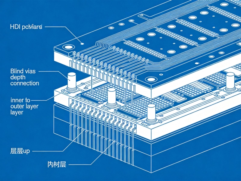
Traditional through-hole via technology consumes significant board area and limits routing density. Hdi Technology addresses these limitations through Microvias, Blind Vias, and Buried Vias. These structures enable higher component density while maintaining the reliability aerospace applications demand.
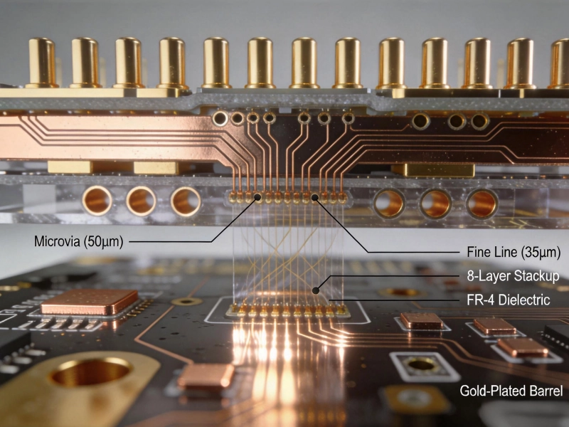
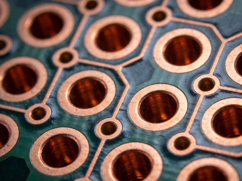
Microvias with diameters below 150 microns provide reliable interconnections when properly designed and manufactured. Their small size reduces thermal expansion stresses compared to larger through-hole vias. This characteristic proves particularly valuable for aerospace applications experiencing extreme thermal cycling.
Stacked Microvia configurations create dense vertical interconnections while preserving routing channels on inner layers. Advanced aerospace designs employ staggered Microvia stacks to distribute mechanical stress and prevent via cracking under thermal load.
Every gram matters in aerospace applications. Launch costs typically exceed $10,000 per kilogram to low Earth orbit. HDI technology enables significant size and weight reductions compared to conventional PCB designs. Smaller boards require less support structure and occupy less volume in spacecraft compartments.
Component Miniaturization permitted by HDI routing density further reduces system mass. Fine-pitch ball grid arrays and chip-scale packages mount directly on Hdi Boards, eliminating the need for larger, heavier component packages.
Material selection fundamentally determines HDI board performance and reliability. Aerospace applications impose stringent requirements beyond standard commercial specifications.
Aerospace Hdi Boards typically employ high-Tg polyimide or epoxy-based laminates. Glass transition temperatures exceeding 180°C ensure dimensional stability across the operational temperature range. Low coefficients of thermal expansion minimize stresses on solder joints and via structures during thermal cycling.
High-modulus materials resist deformation under mechanical load. This characteristic proves essential for boards mounted in vibration-prone locations such as engine compartments or landing gear systems. Materials qualified to Ipc-4101 slash sheets provide baseline performance guarantees.
NASA and ESA maintain strict outgassing requirements for materials used in space applications. The ASTM E595 test measures total mass loss and collected volatile condensable materials. Acceptable materials demonstrate total mass loss below 1.0% and collected volatile condensable materials below 0.10%.
Polyimide materials generally meet these requirements while providing excellent thermal and mechanical properties. Some advanced epoxy formulations also achieve space qualification. Material selection must consider both outgassing characteristics and long-term radiation resistance.
Copper foil quality significantly impacts via reliability and Signal Integrity. Low-profile copper foils provide better adhesion to dielectric materials while maintaining consistent conductor geometry. For aerospace Hdi Applications, electrodeposited copper with controlled grain structure ensures consistent etching behavior and reliable microvia plating.
Very-low-profile and ultra-low-profile copper foils minimize conductor losses at microwave frequencies. This consideration becomes increasingly important as aerospace systems incorporate higher-frequency communications and radar capabilities.
Aerospace HDI design rules exceed commercial specifications to ensure mission reliability. These requirements address via structures, trace geometries, and layer stackup considerations.
Aerospace HDI designs typically specify microvia aspect ratios below 0.6:1. This conservative ratio ensures reliable plating throughout the via barrel. Laser-drilled microvias achieve better aspect ratio control than mechanically drilled holes, making them preferred for aerospace applications.
Capture pad diameters must accommodate registration tolerances while providing sufficient Annular Ring. Typical aerospace designs require minimum annular rings of 50 microns for microvias and 75 microns for Buried Vias. These dimensions account for layer-to-layer misalignment during lamination.
Via stacking rules prevent reliability issues in multilayer configurations. Stacked Microvias require filled and planarized underlying vias to prevent void formation. Staggered via configurations distribute thermal and mechanical stress more effectively than direct stacking.
Fine-line geometries enable dense routing in aerospace HDI boards. Current manufacturing capabilities support 50-micron traces and spaces in production volumes. Advanced facilities achieve 25-micron features for specialized applications.
Trace width consistency proves critical for controlled impedance applications. Aerospace communications and radar systems require precise Impedance Control, typically ±10% or better. Manufacturing processes must maintain trace width variations below ±10% to achieve these tolerances.
Symmetric layer stackups minimize warpage during thermal cycling. Aerospace HDI designs typically employ even layer counts with balanced copper distribution. Core and prepreg thicknesses require careful selection to achieve target overall board thickness while maintaining manufacturability.
Ground and power plane placement affects both electrical performance and Thermal Management. Strategic plane placement provides shielding for sensitive signals while facilitating Heat Dissipation from high-power components.
Aerospace Hdi Manufacturing demands exceptional process control. Each fabrication step requires monitoring and documentation to ensure consistent quality.
UV and CO2 laser systems create microvias with precise depth control. The Laser Drilling process must account for copper thickness variations and dielectric properties. In-process inspection verifies via diameter and positioning accuracy.
Desmear processes remove resin smear from via walls while preserving dielectric integrity. Plasma desmear provides superior results for high-reliability applications, ensuring complete removal of drilling debris without over-etching.
Microvia plating presents significant challenges due to aspect ratio effects. Electroless copper deposition provides uniform seed layer coverage. Pulse plating techniques achieve better copper distribution within high-aspect-ratio vias.
Copper thickness requirements typically specify 25 microns minimum in via barrels and 35 microns on surface traces. Cross-section analysis verifies plating thickness and uniformity. Thermal stress testing validates plating adhesion and ductility.
Sequential Lamination processes build multilayer HDI structures. Each lamination cycle must achieve complete resin flow without creating voids or delamination. Temperature and pressure profiles require optimization for specific material combinations.
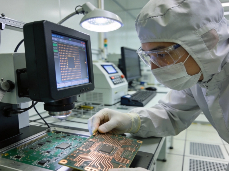
Post-lamination inspection identifies internal defects before additional processing. X-ray Inspection verifies via alignment and Layer Registration. Cross-section analysis confirms material consolidation and via integrity.
Aerospace HDI boards undergo extensive testing beyond standard electrical verification. These tests validate reliability under mission-relevant environmental conditions.
Flying probe and bed-of-nails testers verify continuity and isolation. Impedance testing validates controlled impedance structures. High-potential testing confirms dielectric integrity.
Time-domain reflectometry identifies impedance discontinuities and signal path defects. This testing proves particularly valuable for high-speed aerospace signal paths.
Thermal cycling tests subject boards to repeated temperature extremes. Typical aerospace qualification requires 500 to 1000 cycles between -55°C and +125°C. Resistance monitoring during cycling detects via and trace degradation.
Random vibration testing simulates launch and operational environments. Test levels typically range from 10 to 20 Grms depending on mounting location and vehicle characteristics. Post-vibration inspection identifies mechanical defects.
Highly accelerated stress testing provides rapid reliability assessment. HAST exposes boards to elevated temperature and humidity conditions while applying bias voltage. This testing accelerates failure mechanisms that might otherwise require years of operational testing.
Sample boards undergo cross-section analysis to verify internal construction. Microscopic examination confirms via plating quality, Layer Registration, and material consolidation. Scanning electron microscopy identifies microscopic defects invisible to optical inspection.
Microsectioning evaluates plating thickness, dielectric spacing, and copper grain structure. These analyses validate manufacturing process control and provide data for continuous improvement.
Aerospace applications require complete traceability from raw materials through finished product. Quality management systems must document every manufacturing step and material lot.
AS9100 quality management provides the foundation for aerospace Pcb Manufacturing. Additional requirements from specific programs may impose supplementary controls. Manufacturing facilities must maintain NADCAP accreditation for special processes such as plating and welding.
Material traceability extends to base laminates, copper foils, prepreg materials, and chemical processes. Lot numbers link finished boards to specific material batches, enabling investigation if field issues arise.
HDI technology enables the miniaturization and performance that modern aerospace systems demand. However, realizing these benefits requires rigorous attention to material selection, design practices, and manufacturing controls. Mission-critical applications leave no margin for error.
Successful aerospace HDI programs begin with clear requirements definition and end with comprehensive qualification testing. Every manufacturing step requires careful control and documentation. The investment in quality pays dividends through mission success and long-term reliability.
As aerospace systems continue evolving toward greater capability in smaller packages, HDI technology will play an increasingly central role. Manufacturers mastering aerospace HDI requirements position themselves at the forefront of this critical industry segment.
Designing HDI Boards to Withstand Extreme Aerospace EnvironmentsJuly/22/2026
High-Reliability Interconnects for Satellite and Space CommunicationSeptember/18/2026
The Challenge of Plating and Filling Microvias in HDI ProductionJuly/26/2026
What is High Density Interconnect (HDI) PCB?May/28/2026
Understanding HDI Terminology: A Glossary for EngineersAugust/03/2026
The Importance of Electrical Testing for Microvia ReliabilityJuly/09/2026

How HDI Technology Supports Advanced Driver Assistance Systems (ADAS)June/25/2026
High-Reliability HDI Solutions for PLCs and Motor DrivesSeptember/16/2026