Open Nav

If you've been working with modern electronics, you've probably heard the term Hdi Pcb thrown around a lot. But what exactly does it mean, and why is it becoming so important in today's compact devices? In this guide, we'll break down everything about High Density Interconnect (HDI) PCB — from what it actually is, to how it's manufactured, and why tech giants like Apple and Samsung rely on it for their smartphones and Wearables. Whether you're an engineer, a procurement manager, or just someone curious about Pcb Technology, this article got you covered.
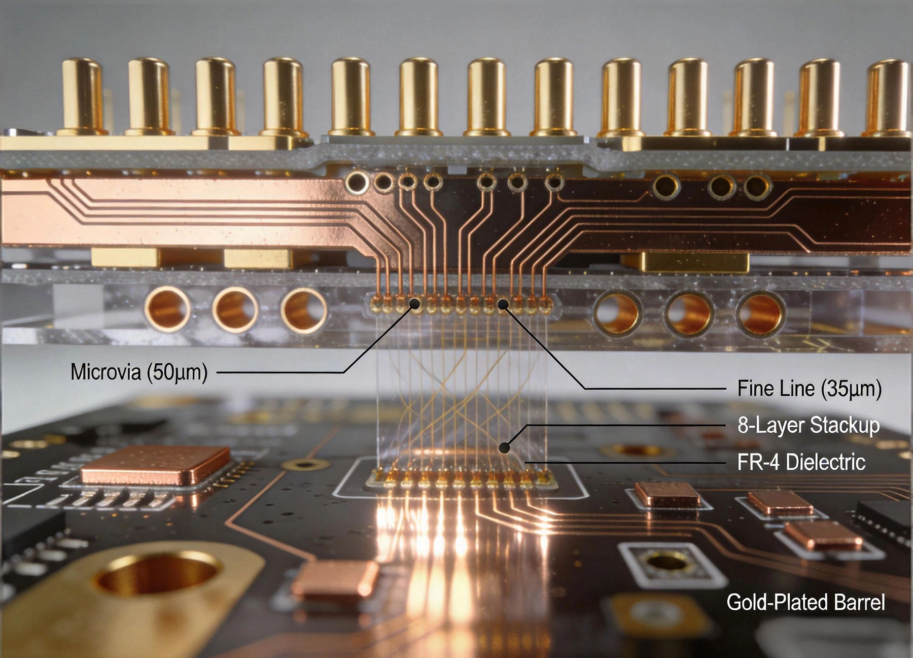
A High Density Interconnect PCB is simply a printed circuit board that packs more functionality into a smaller space compared to traditional boards. The magic behind this is its use of Microvia Technology and finer trace widths, which allows designers to route more signals in less area. Think about the difference between a country road and a 10-lane highway — both get you from point A to point B, but one handles way more traffic in a fraction of the space.
The IPC (Institute for Printed Circuits) defines Hdi Boards as those featuring a higher wiring density per unit area compared to conventional PCB technologies. In plain English, this means more components, more connections, and smaller board sizes — all at once. The demand for Hdi Boards has exploded since the early 2000s, driven primarily by the smartphone revolution. When phone manufacturers started competing to make devices thinner and more powerful, traditional through-hole Pcb Technology just couldn't keep up with the space requirements.
Consider this: a smartphone from 2010 might have used a 4-layer PCB. Today's flagship smartphones routinely use 8 to 12-layer HDI PCBs with Microvia structures, all while fitting into a case that's thinner than a pencil. This isn't just incremental improvement — it's a fundamental shift in how we build electronic devices.
Not all HDI PCBs are created equal. There are several distinct types, each with its own advantages and trade-offs. Understanding these differences helps when you're deciding which configuration best suits your project.
This is the simplest form of HDI. It uses a single layer of prepreg on each side of the core, with through vias connecting all layers and Microvias connecting the outer layers to the adjacent inner layers. For many consumer electronics applications, 1-N-1 provides the right balance of density and cost. It's often the go-to choice for mid-range smartphones and tablets where moderate Miniaturization is needed.
Stepping up in complexity, 2-N-2 uses two buildup layers on each side of the core. This configuration offers higher routing density and is common in more advanced applications. The additional buildup layers mean more routing channels, which translates to better Signal Integrity and the ability to handle more complex designs.
Also known as any layer interconnect HDI, this is the most advanced configuration where all layers are interconnected using Microvias. Every single layer can connect to any other layer through these microstructures, giving designers maximum flexibility. Apple's iPhone series famously uses any layer Hdi Technology, which contributes significantly to the phone's remarkable thinness and dense component placement.
| Type | Buildup Layers | Density Level | Typical Applications | Cost Factor |
|---|---|---|---|---|
| 1-N-1 | 1 layer each side | Moderate | Tablets, mid-range phones | 1.0x (baseline) |
| 2-N-2 | 2 layers each side | High | High-end smartphones, medical devices | 1.5-2.0x |
| Any Layer | All layers interconnected | Very High | Flagship devices, Wearables | 2.0-3.0x |
At the heart of every Hdi Pcb is the Microvia. Unlike traditional through-hole vias that drill all the way through the board, microvias are tiny holes that only connect adjacent layers. This might not sound like a big deal, but it changes everything about how you can design a board.
Traditional vias consume what's called "via stub" — the portion of the hole that extends beyond the connection point. These stubs act like antennae and cause signal reflection, especially in high-frequency applications. Microvias eliminate this problem because they only go where they need to go. The result is cleaner signal transmission and better electrical performance, particularly important in 5G communication and high-speed digital designs.
There are two primary types of microvias you'll encounter:
Manufacturing HDI PCBs is significantly more complex than producing standard multilayer boards. Here's a simplified walkthrough of the key steps involved:
It all starts with a core substrate, typically made of FR-4 or a high-speed material like Rogers. The inner layers are imaged and etched, similar to standard PCB production. But here's where the precision really matters — the line widths and spacing in HDI boards are much tighter, often down to 50 microns or less. Any variation in the etching process can cause opens or shorts, so strict process control is essential.
This is where Hdi Pcb Manufacturing really separates itself from conventional processes. In Sequential Lamination, the core is built up layer by layer. After each pair of buildup layers is pressed and cured, the board moves to the next stage. Each cycle involves:
Microvias are typically created using CO2 or UV Laser Drilling systems. The laser removes the Dielectric Material without damaging the underlying copper pad — a precision operation that requires sophisticated optical systems and tight process controls. After drilling, the holes go through a desmear process to remove any resin residue, followed by Copper Plating to create the conductive connection.
Once all layers are built up, the board goes through final processing including solder mask application, surface finish (ENIG, OSP, or Immersion Tin), silk screening, and electrical testing. HDI boards undergo more rigorous testing than standard boards because the consequences of a microvia failure can be catastrophic in mission-critical applications.
Why are so many electronics manufacturers switching to HDI PCB technology? The advantages are substantial and span multiple dimensions:
Studies show that Hdi Technology can reduce board area by up to 40% compared to equivalent multilayer designs. For mobile devices where every square millimeter matters, this is a game-changer. A smartphone that would require a 6-layer Traditional Pcb might achieve the same functionality in just 4 layers using HDI technology.
Shorter electrical paths mean faster signal transmission and reduced latency. The elimination of via stubs in microvia designs also improves Signal Integrity at high frequencies. For 5G applications and high-speed data buses (think PCIe 5.0 and DDR5 memory interfaces), HDI boards aren't just preferable — they're often mandatory.
Counterintuitively, High Density Interconnect PCBs can actually improve Thermal Performance. The microvia structures create more efficient heat conduction paths from hot components to thermal ground planes. Combined with the ability to use metal core substrates in HDI constructions, this makes HDI a viable option for high-power applications.
With more routing layers and the ability to place vias anywhere (rather than just in dedicated via areas), designers have significantly more freedom. This translates to better component placement, shorter trace lengths for critical nets, and the ability to implement complex routing topologies that would be impossible on traditional boards.
Hdi Pcb Technology has become the backbone of modern consumer electronics, but its applications extend far beyond smartphones:
Designing for Hdi Pcb Manufacturing requires a different mindset compared to traditional board design. Here are some practical considerations we've learned from working with HDI technology:
High-speed signals need careful routing in HDI designs. Use differential pairs for critical signals and maintain consistent impedance throughout the routing. The shorter trace lengths achievable with HDI actually help here — you're less likely to encounter the impedance discontinuities that plague longer runs on traditional boards.
Dense component placement means Heat Dissipation becomes more challenging. Plan Thermal Vias near power components and consider thermal relief patterns around pads. If your design includes BGAs with many pins, thermal balls connected to ground planes through microvias can dramatically improve Thermal Performance.
Always work with your HDI PCB manufacturer to understand their specific capabilities. Minimum line/space, microvia capture pad size, and registration tolerances vary between fabs. A good rule of thumb: design to 80% of the manufacturer's stated minimum capabilities to ensure acceptable yields. Don't try to push every parameter to its theoretical limit on the same board — there's a cumulative effect on manufacturability.
It's no secret that HDI Pcb Manufacturing costs more than traditional multilayer boards. The laser drilling, Sequential Lamination, and tighter process controls all add to the production expense. However, the total cost picture is often more nuanced than the unit price suggests.
When you factor in the board area savings, reduced layer count, and potentially simpler mechanical packaging, HDI can actually reduce your overall system cost. A single smaller HDI board might replace two or three larger traditional boards, eliminating inter-board connectors and reducing assembly complexity. In high-volume consumer electronics where these savings multiply across millions of units, the economics are clear.
For lower-volume industrial or medical applications, the calculation shifts. Here, the reliability benefits and performance advantages of HDI often justify the premium, especially when the alternative would be a much larger, heavier assembly. The key is to evaluate HDI adoption on a total system cost basis, not just the PCB unit price.
Whether you're designing a next-generation smartphone or a compact medical device, our engineering team has the expertise to bring your Hdi Pcb Design to life. From prototype to high-volume production, we support all HDI configurations including 1-N-1, 2-N-2, and any layer HDI.
Current manufacturing capabilities allow microvia diameters as small as 50 microns (0.05mm), though 75-100 microns is more common for production. The choice depends on your manufacturer's laser drilling capability and the board's layer count. Smaller microvias mean higher manufacturing cost and lower yields, so choose the largest size that meets your routing requirements.
The main differences are the use of microvias instead of through-hole vias, finer trace widths and spacing, and sequential lamination for buildup layers. Traditional multilayer PCBs drill through the entire board stack for every via, while HDI uses laser-drilled microvias that only connect adjacent layers. This gives HDI better electrical performance, smaller size, and more design flexibility.
Yes, absolutely. Flexible and rigid-flex HDI boards are increasingly common, particularly in foldable smartphones and wearables. These use polyimide substrates instead of FR-4 and require specialized materials and processes. The same HDI principles (microvias, fine lines, sequential lamination) apply, but with additional considerations for flexural stress and bend radius.
HDI PCBs typically require 10-21 days for production, compared to 5-10 days for standard multilayer boards. The sequential lamination process alone takes multiple days because each buildup layer must be fully cured before proceeding to the next. For prototype runs, some manufacturers offer expedited services at premium pricing.
ENIG (Electroless Nickel Immersion Gold) is the most common surface finish for HDI boards because it provides a flat, coplanar surface ideal for fine-pitch components and offers excellent shelf life. Immersion Silver and OSP (Organic Solderability Preservative) are also widely used, particularly for cost-sensitive applications. For high-reliability aerospace and medical applications, Hard Gold plating may be specified for edge connectors.
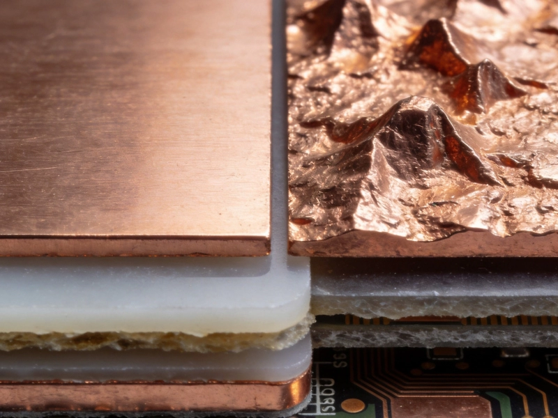
Understanding the Role of Copper Foil Roughness in Signal IntegritySeptember/23/2026
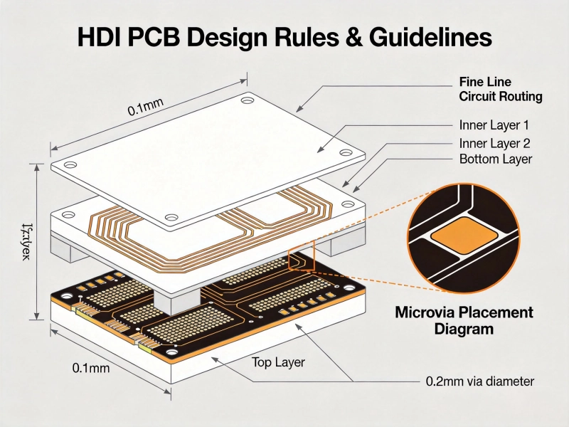
Essential HDI PCB Design Rules for Beginners and ExpertsMay/28/2026
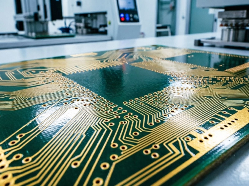
Selecting the Right Dielectric Materials for High-Performance HDI PCBsJune/05/2026
An Introduction to ABF (Ajinomoto Build-up Film) for Advanced HDIJuly/27/2026
Managing Layer-to-Layer Registration Accuracy in Multilayer HDIOctober/09/2026
FR-4 vs. High-Tg Materials: What Works Best for HDI Applications?July/07/2026
Why Low Loss Materials are Critical for High-Speed HDI DesignsSeptember/01/2026
Using HDI Technology in Solar Inverters and ConvertersOctober/14/2026