Open Nav

Heat is the enemy of electronics. Every electronic component converts some electrical energy into heat, and as components get smaller, more powerful, and more densely packed, managing that heat becomes one of the most critical challenges in high-density Pcb Design. Get Thermal Management wrong, and your product fails prematurely — sometimes catastrophically. Get it right, and you deliver reliable performance that meets or exceeds expectations. This guide covers every major Thermal Management strategy for PCBs, from basic Heat Dissipation techniques to advanced cooling solutions for the most demanding applications.
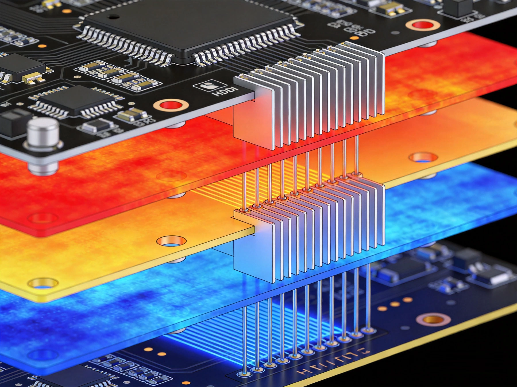
The electronics industry has been on a relentless drive toward Miniaturization. Components that once occupied square centimeters now fit into millimeter-scale packages. A smartphone processor that would have required a dedicated heat spreader a decade ago now dissipates 5-10 watts from a chip smaller than a fingernail. This density creates thermal challenges that conventional Pcb Design approaches simply cannot solve.
High-density Interconnect (HDI) PCBs compound the challenge further. The very thin dielectrics that enable HDI's Miniaturization also make thermal management more difficult. Heat generated at the component level must find a path to the environment through increasingly thin layers of substrate material. And when multiple hot components sit millimeters apart on a dense HDI board, the thermal interaction between them creates hotspots that single-component thermal analysis misses entirely.
Beyond reliability, thermal management affects performance directly. Most semiconductor devices exhibit reduced switching speed and increased leakage current as temperature rises. A processor that delivers 3.5 GHz at 70°C might drop to 3.0 GHz at 100°C. Thermal throttling — where the chip automatically reduces clock speed to prevent overheating — has become a common feature precisely because thermal management at the system level remains challenging.
Before diving into specific strategies, it's essential to understand how heat moves through a PCB thermal management system. Heat transfers through three mechanisms, all of which come into play in a typical PCB:
Heat flowing through solid materials — the copper traces, the substrate, the component leads, and the solder joints. The rate of conductive heat transfer depends on the material's Thermal Conductivity (measured in W/mK). Copper has Thermal Conductivity around 386 W/mK, while standard FR-4 substrate is only about 0.3 W/mK. This massive difference means heat follows copper paths, not dielectric paths.
Heat transfer from a solid surface to a moving fluid (air or liquid). Natural convection occurs when heated air rises naturally; forced convection uses fans or liquid circulation to accelerate the process. Convection is typically the dominant heat removal mechanism from the board surface.
Heat transfer through electromagnetic waves. At typical PCB operating temperatures (below 100°C), radiation accounts for only a small fraction of total heat transfer — typically less than 10%. Its contribution becomes more significant in high-temperature environments or in vacuum applications where convection is absent.
| Material | Thermal Conductivity (W/mK) | Application Notes |
|---|---|---|
| Copper | 386 | Primary heat conduction path in PCB |
| Aluminum (core) | 180-220 | Metal core PCB substrates |
| Standard FR-4 | 0.25-0.35 | Poor conductor, limits heat flow |
| High-Tg FR-4 | 0.30-0.40 | Slightly better than standard FR-4 |
| Hydrocarbon Ceramic | 0.60-0.80 | Better thermal performance |
| Polyimide | 0.30-0.50 | Similar to FR-4 |
| Thermal Via Array | 5-50 (effective) | Depends on fill factor and plating |
| Thermal Pad (direct mount) | Variable | 取决于界面材料和接触压力 |
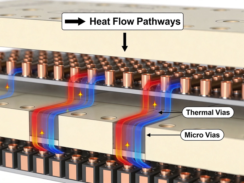
Thermal Vias are the most fundamental and widely used thermal management technique in PCB design. A thermal via is simply a via — a plated-through hole — placed to conduct heat from a component pad to an internal or external plane layer, or from one surface of the board to the other. They're simple to implement, require no additional components, and work with standard Pcb Manufacturing processes.
Heat from a component conducting pad flows through the solder joint into the pad on the PCB surface. From there, it spreads through the copper trace and pad structure and enters the thermal via array. The Copper Plating inside the via provides a high-conductivity path (via copper has thermal conductivity around 386 W/mK) that conducts heat deep into the board structure, where it can spread through planes or reach the opposite surface for convection cooling.
The interface between a component and the PCB is often the critical thermal bottleneck. Even with perfect thermal vias below, if the thermal pad doesn't make good contact with the board, heat accumulates at the package. Thermal pad design addresses this bottleneck directly.
For the highest power components, direct mounting to external heatsinks provides the best thermal path. This requires:
Copper planes in a Multilayer Pcb are not just for electrical return current and power distribution — they're also excellent heat spreaders. With thermal conductivity 1000x better than FR-4, copper planes can spread heat across the entire board, reducing local hotspots and increasing the effective area available for convective cooling.
When you need thermal isolation between components (for example, to prevent heat from a power regulator affecting a temperature sensor nearby), use split thermal planes with controlled thermal paths between them. You can create thermal bridges using controlled-width copper traces rather than solid connections, which limits heat flow while maintaining electrical isolation.
The substrate material determines the baseline thermal resistance of your board. For high-density PCB thermal management, material selection can make a significant difference in thermal performance.
Higher thermal conductivity materials typically cost more and may have different electrical properties. For example, metal core PCBs have higher capacitance between layers, which affects Impedance Control for high-speed signals. Always evaluate thermal benefits against electrical performance requirements and cost constraints.
For very high power densities, passive thermal management — thermal vias, spreading planes, and heatsinks — cannot remove heat fast enough. Active cooling uses forced convection or liquid cooling to dramatically increase heat removal capacity.
For the highest power applications, liquid cooling provides heat removal capacity 10-100x that of forced air. Options include:
Component placement significantly impacts thermal performance, often more than any single thermal management technique. Getting placement right from the start avoids costly redesigns later.
For complex boards with multiple power components, perform Thermal Simulation or analysis that accounts for thermal coupling between components. Individual component thermal resistance specifications only tell part of the story — when components are placed close together, their thermal influence combines.
The most effective thermal management strategy is to reduce heat generation in the first place. Power dissipation design addresses thermal issues through circuit and system design, not just PCB layout.
Components are often specified with a TDP rating — the maximum sustained power they are expected to dissipate under typical operating conditions. However, peak power during transient operations (burst mode, rapid data processing) can significantly exceed TDP. Design your thermal management for peak power, not TDP, or implement thermal throttling to protect against transients.
Thermal management in smartphones presents unique challenges: extreme miniaturization, battery constraints limiting active cooling, aesthetic constraints limiting heatsink size, and user comfort limits on surface temperature. Common approaches include graphite heat spreaders (thin, flexible, high thermal conductivity), vapor chamber cooling for flagship devices, and aggressive software-based thermal throttling that prioritizes sustained performance over peak performance.
Automotive applications face extreme thermal environments: under-hood temperatures can exceed 125°C, while dash and infotainment areas experience significant solar heating loads. Automotive PCBs require extended temperature range components (Grade 1: -40°C to +125°C operating range) and robust thermal design margins. Many automotive ECUs use forced-air cooling or liquid cooling loops connected to the engine cooling system.
High-performance networking switches, routers, and servers dissipate hundreds to thousands of watts. These applications use sophisticated thermal management: direct liquid cooling (cold plates on processor and ASIC packages), immersion cooling (entire PCB submerged in dielectric coolant), and row-based cooling with precision airflow management.
LED thermal management is critical because LED efficiency and lifespan decline sharply with temperature. A 10°C increase above rated operating temperature roughly doubles degradation rate. LED PCBs typically use metal core substrates (MCPCB) with thermal vias connecting LED packages directly to the aluminum base, which mounts to a heatsink or luminaire housing.
Medical devices have stringent thermal limits for patient contact (surface temperature limits for skin-contact devices) and must maintain accuracy of sensing circuits whose performance varies with temperature. Thermal design must balance electronic thermal requirements against patient safety and measurement accuracy constraints.
A thermal design is only as good as its validation. Thermal testing confirms that your design meets thermal requirements under all expected operating conditions.
Our engineering team specializes in thermal management for high-density PCBs across consumer electronics, automotive, industrial, and medical applications. We offer thermal simulation, design review, and optimization services to ensure your product meets thermal and reliability requirements. Contact us today to discuss your thermal challenges.
The answer depends on the thermal power dissipation, the allowable temperature rise, and the target layer. As a starting point, a typical guideline for processors dissipating 3-5W is 25-50 thermal vias in a grid pattern directly under the thermal pad. For lower-power components (1-2W), 9-16 vias may suffice. For high-power devices (>10W), you may need 100+ vias or direct liquid cooling integration. Always verify with thermal simulation or measurement against your specific requirements.
Thermally, there's no inherent difference — a thermal via is just a standard via used for thermal purposes. The distinction is in placement and design intent. Thermal vias are typically placed under thermal pads, arranged in a dense grid, and connected to thermal spreading planes. Standard vias are used for electrical signal routing and may be placed anywhere on the board. From a manufacturing perspective, they're identical — the same drilling, plating, and processing steps apply.
For thermal pads that need to conduct heat, never use thermal relief spokes — these add thermal resistance at exactly the point where you want maximum heat transfer. Connect the thermal pad directly to the thermal via array or spreading plane with full copper connection. Thermal relief is appropriate for signal pads and low-power component connections where the minor thermal resistance doesn't matter, but thermal relief on thermal pads defeats their purpose.
Thinner boards have higher thermal resistance through the substrate (less cross-sectional area for heat flow), but may have better convective cooling from both surfaces if components are on both sides. For single-sided assemblies, a thicker board can actually improve thermal performance by providing more area for heat spreading in the copper planes. The effect is application-specific, but in general, don't reduce board thickness solely for thermal reasons without analysis.
For most applications, thermal vias are the most cost-effective thermal management technique — they require no additional components, use standard manufacturing processes, and can significantly reduce thermal resistance. A well-designed via array can reduce thermal resistance by 5-10x compared to no thermal vias. Adding copper spreading planes and optimizing component placement are also essentially free in terms of PCB cost. Active cooling (fans, liquid cooling) and specialized materials (metal core, ceramic substrates) add significant cost and should be reserved for applications where passive thermal management cannot meet requirements.
Thermal cycling causes fatigue in solder joints, vias, and PCB materials. For products that experience temperature cycling (automotive, industrial outdoor, aerospace), design for thermal cycling from the start. Use components with adequate thermal cycling ratings, specify high-Tg PCB materials (high-Tg FR-4 or polyimide) that maintain mechanical properties through temperature extremes, ensure thermal via design avoids stress concentration at the pad interface, and consider thermal underfill for large BGAs to distribute thermal expansion mismatch loads. Thermal cycling testing should be part of your reliability qualification program.
How to Use Thermal Simulation Software to Optimize HDI LayoutsJuly/29/2026
Copper Coin and Embedded Heat Sinks: Advanced Cooling for HDIJuly/08/2026
Selecting the Right Dielectric Materials for High-Performance HDI PCBsMay/28/2026
The Role of Thermal Vias in Dissipating Heat from HDI BoardsJune/09/2026
Exploring the 6 Types of HDI Structures: From Type I to Any-LayerAugust/14/2026
The Role of HDI Technology in Wearable Device MiniaturizationJuly/15/2026
Understanding Sequential Lamination in Multi-Step HDI BoardsJuly/03/2026
Conductive Anodic Filament (CAF) Resistance in High-Density BoardsJuly/31/2026