Open Nav

Equally critical is the rigorous testing process. Manufacturers employ Automated Optical Inspection (AOI) and X-ray analysis to detect microscopic defects in fine traces and via structures. To guarantee long-term durability, boards undergo demanding environmental stress tests, such as thermal cycling and mechanical vibration simulations. These tests validate that the High Density Interconnect PCB can withstand real-world operating conditions without failures like layer separation or via fracture, ensuring top-tier performance for complex electronic applications.
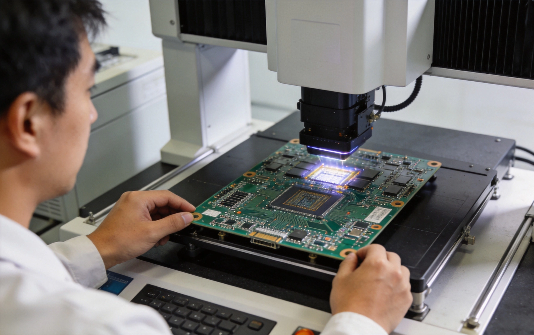
Non-Destructive Testing Techniques for Multilayer HDI PCBsSeptember/29/2026Multilayer High-Density Interconnect (HDI) PCBs form the foundation of modern compact, high-performance electronics including smartphones, medical implants, aerospace systems, and automotive advanced driver assistance systems. With trace widths as small as 25μm, microvias (blind, buried, and stack...
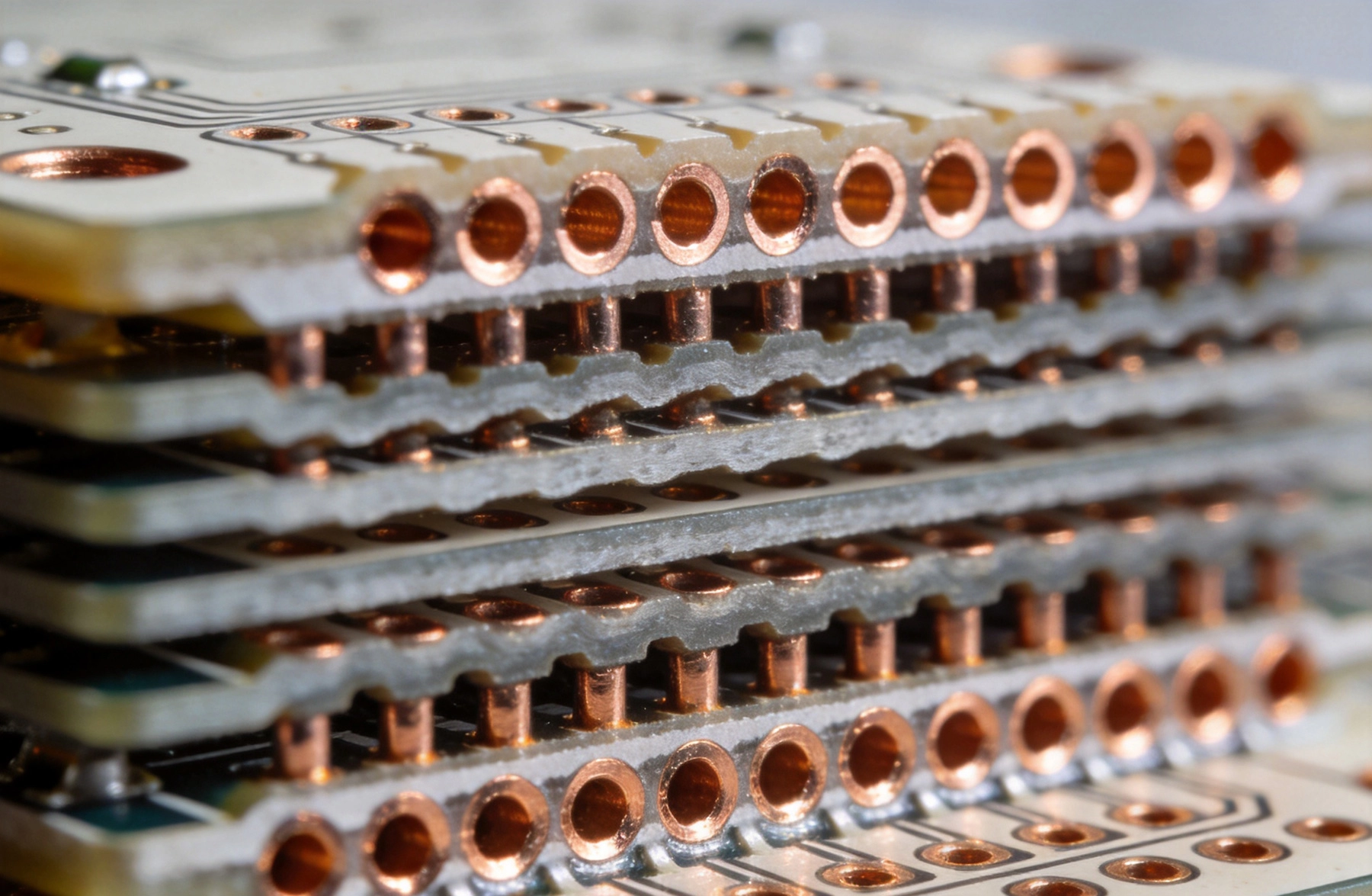
The Art of Microvia Placement: Staggered vs. Stacked ViasSeptember/24/2026As electronics continue their relentless march toward miniaturization, high-density interconnect (HDI) technology has become standard practice rather than exotic exception. And at the heart of every HDI design lies the microvia—those laser-drilled, small-diameter vias that make the interlayer conn...
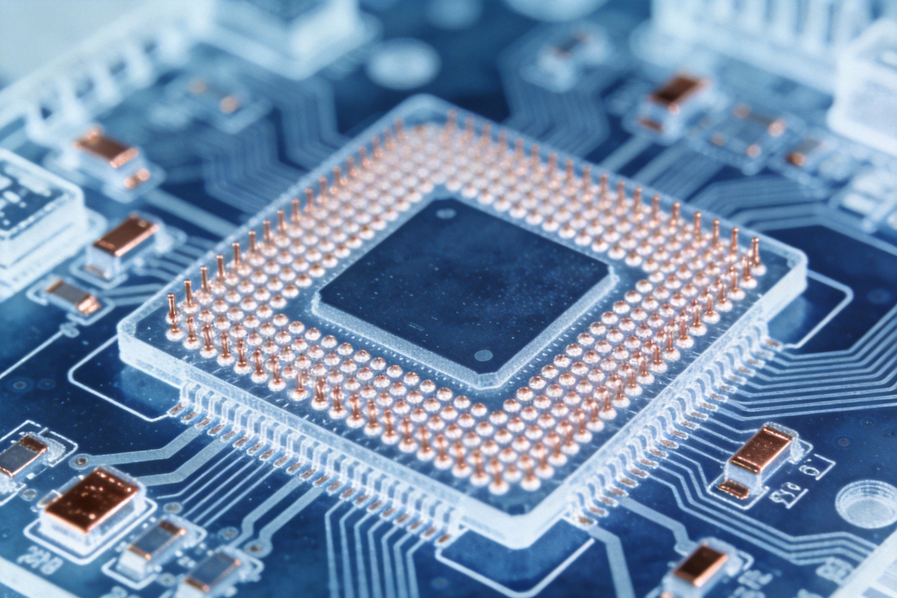
Overcoming the Challenges of Testing Fine-Pitch BGA on HDISeptember/04/2026The semiconductor industry keeps shrinking feature sizes while packing more functionality into each chip. The result: Ball Grid Array packages with pitches of 0.4mm, 0.3mm, and even 0.2mm, mounted on HDI substrates that route signals through microvias and fine traces. This combination delivers rem...
Designing for Manufacturing (DFM): Avoiding Common HDI PitfallsSeptember/02/2026High-Density Interconnect (HDI) PCBs have become the backbone of modern electronics, enabling the miniaturization, performance, and functionality that consumers and industries demand. From smartphones and wearable devices to medical implants and aerospace systems, HDI technology makes it possible ...
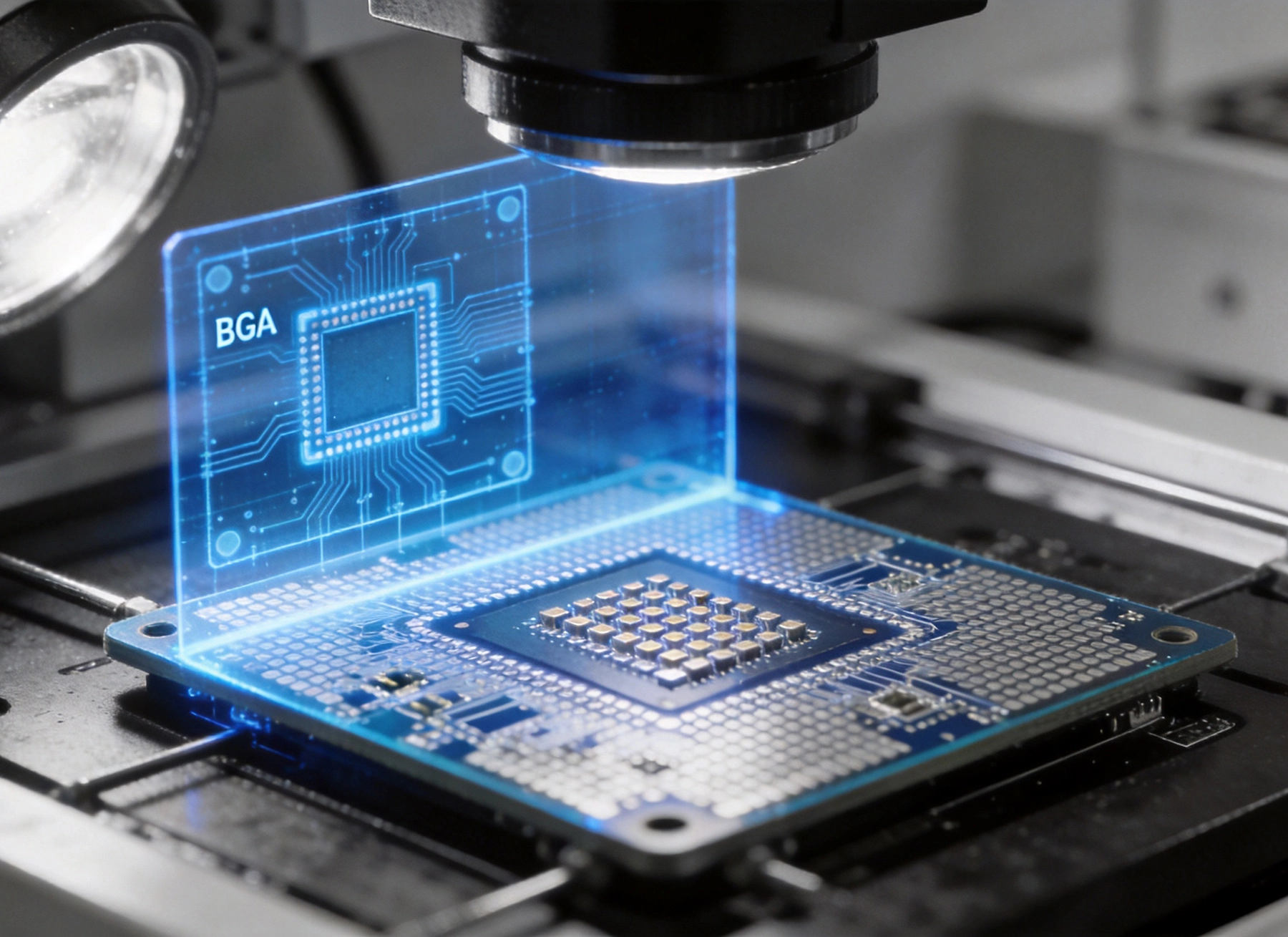
How X-Ray Inspection (AXI) Detects Hidden Defects in HDI BoardsJuly/30/2026High density interconnect boards, commonly called HDI boards, represent the pinnacle of PCB miniaturization. With microvias smaller than a human hair and ball grid array packages hiding hundreds of solder joints beneath a component the size of a fingernail, these boards push manufacturing toleranc...
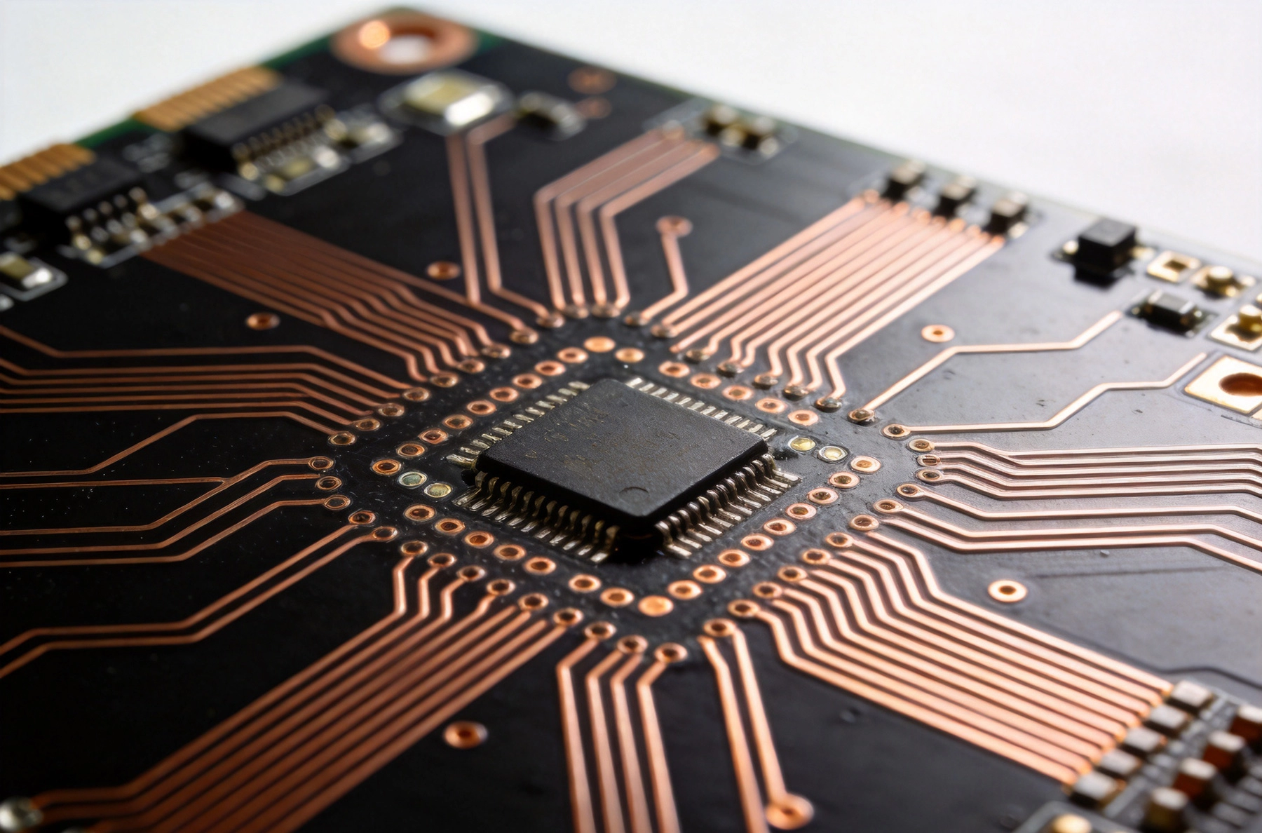
How to Implement Effective Impedance Control in HDI DesignsJuly/28/2026High-density interconnect designs compress more routing into less space, which makes impedance control both more critical and more difficult. The physics of impedance does not change — controlled impedance still depends on trace geometry, dielectric properties, and reference plane distance. What c...
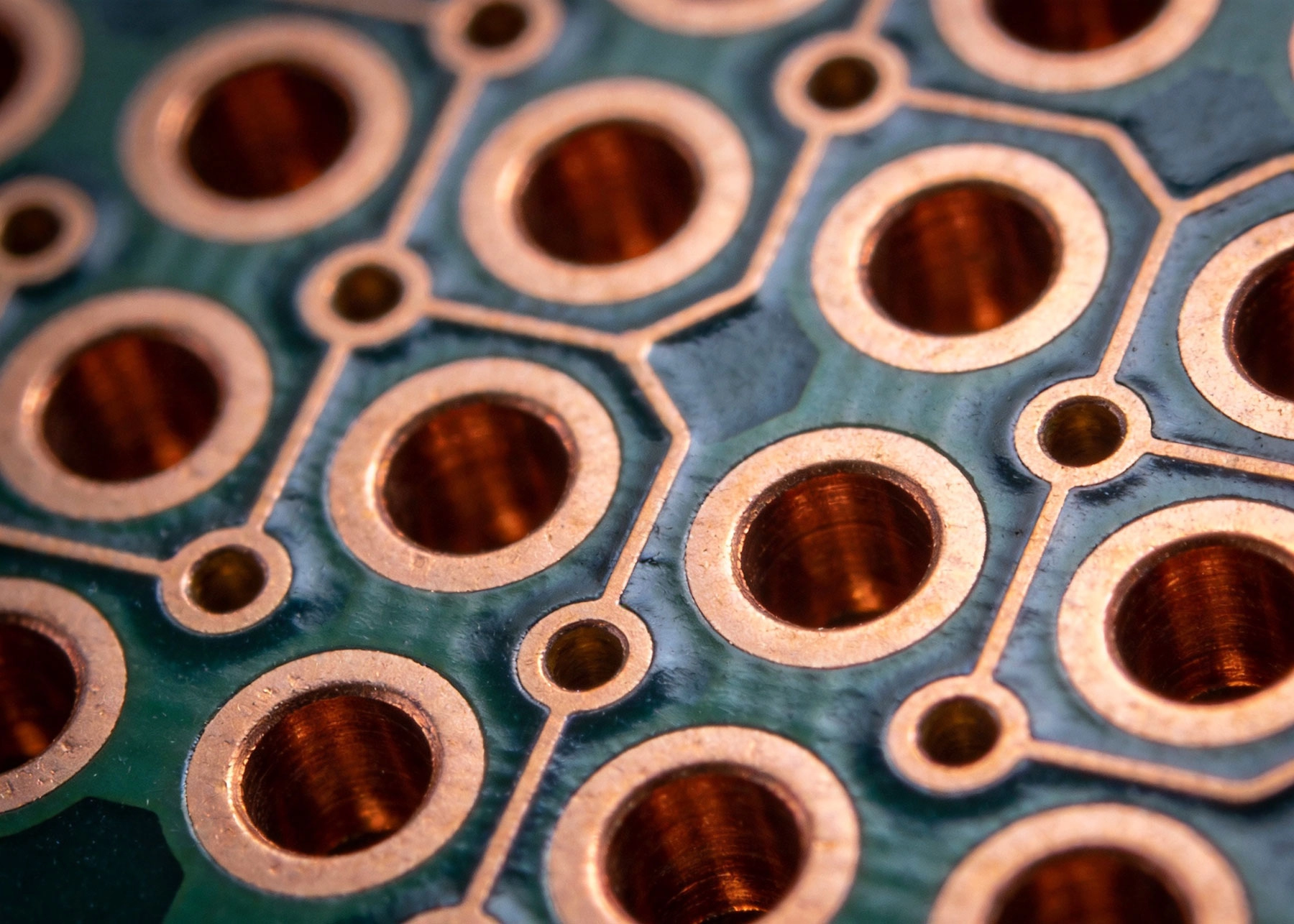
The Importance of Electrical Testing for Microvia ReliabilityJuly/09/2026As PCB technology advances and device geometries shrink, the humble via—the plated hole that connects layers in a printed circuit board—has become one of the most critical and most vulnerable elements in modern electronics. Microvias, defined by the IPC standard as vias with a diameter of 0.15 mil...
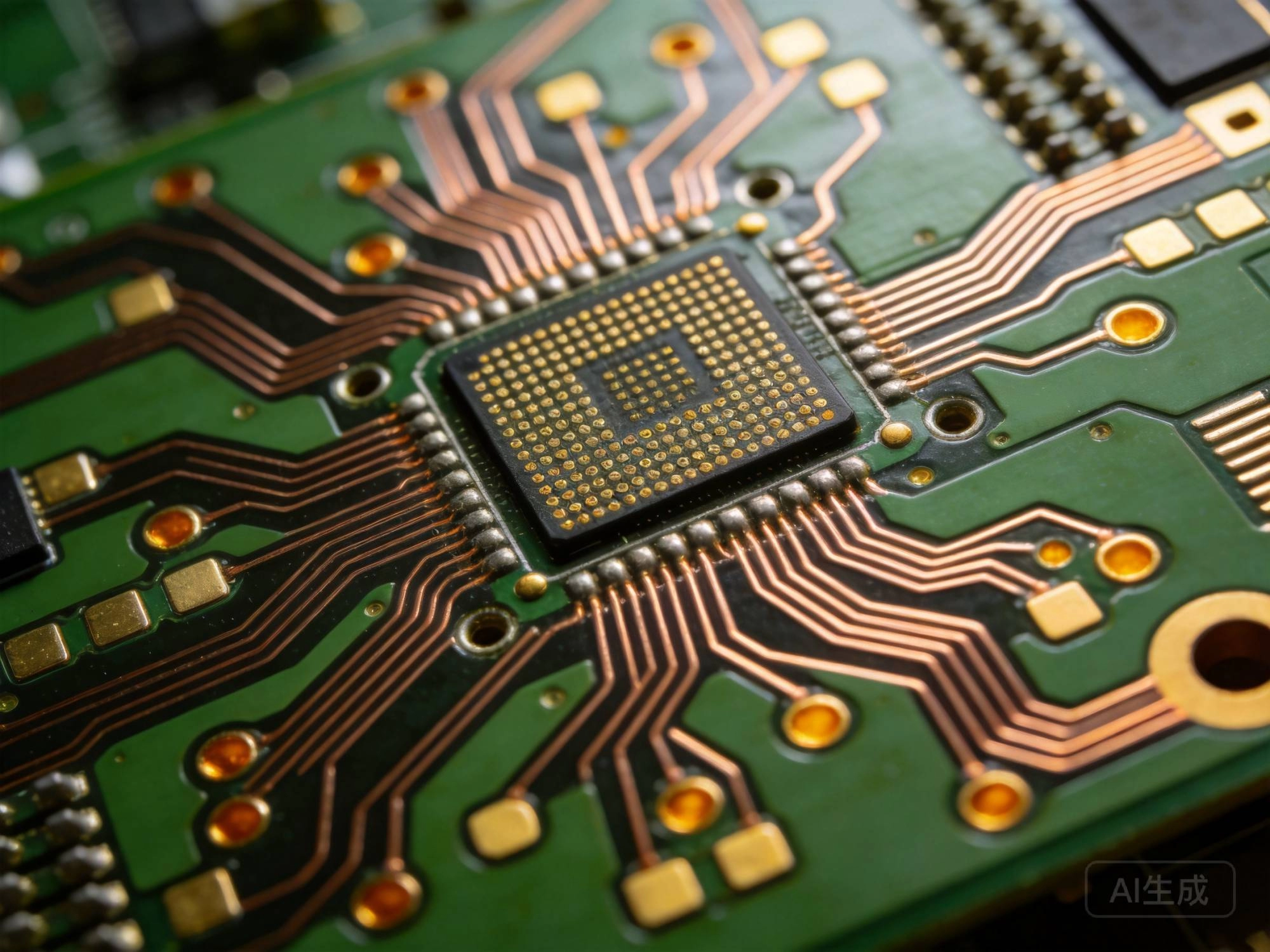
Best Practices for BGA Fanout and Routing in HDI LayoutsJuly/07/2026Ball Grid Array packaging has become the default choice for modern semiconductor devices, from microprocessors and FPGAs to memory chips and wireless modules. The technology delivers unmatched pin density—today's high-pin-count devices exceed 2,000 connections in packages smaller than a thumbnail....
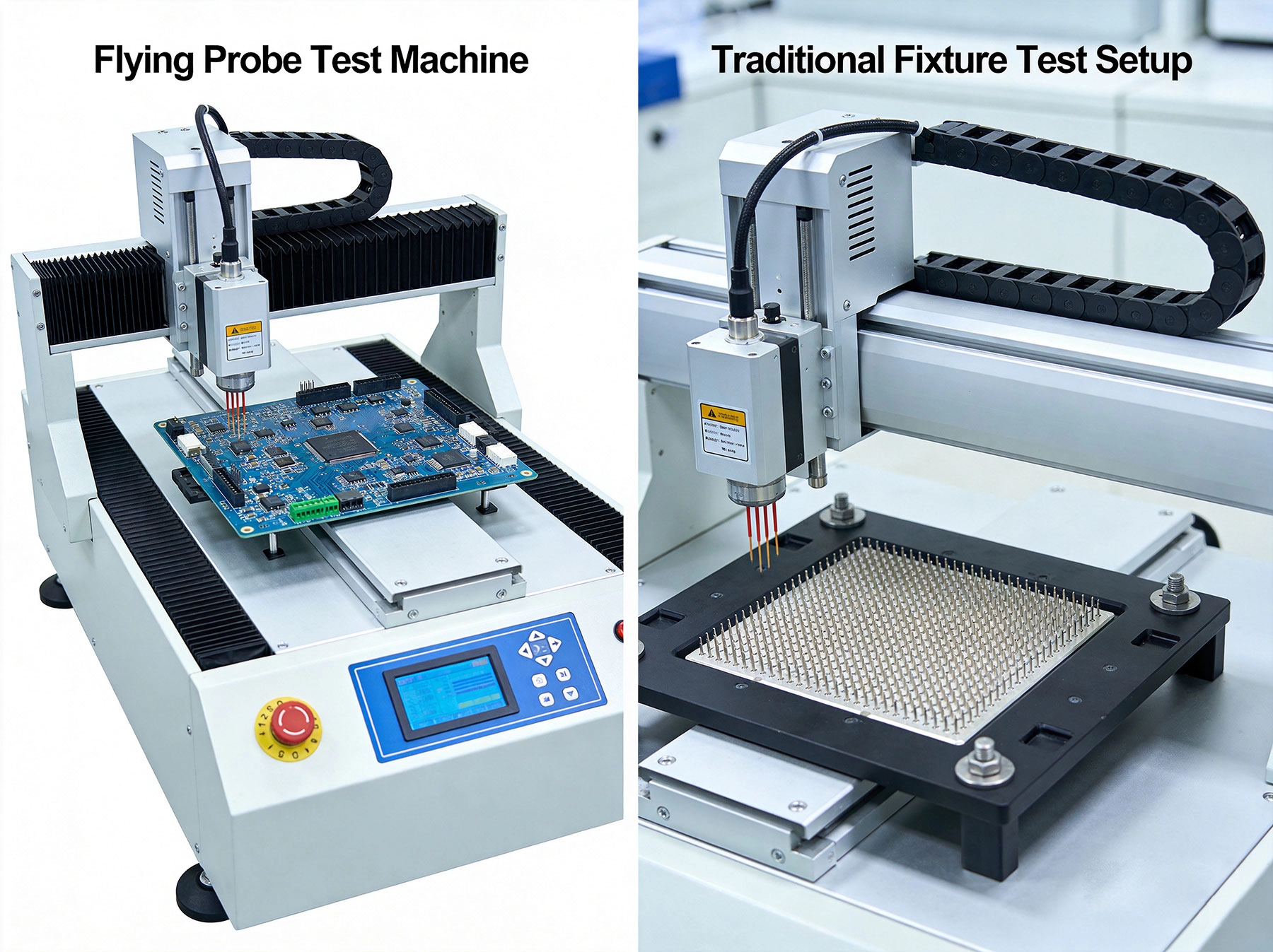
Flying Probe vs. Fixture Testing: Which is Best for HDI PCBs?June/11/2026IntroductionWhen it comes to testing High Density Interconnect (HDI) PCBs, the stakes are higher than ever. These advanced circuit boards feature ultra-fine traces, micro-vias, and component densities that push the boundaries of traditional testing methodologies. Choosing the right testing app...
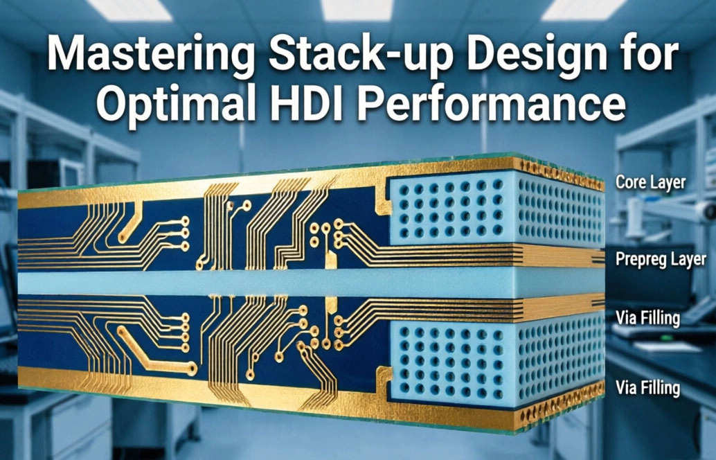
Mastering Stack-up Design for Optimal HDI PerformanceJune/08/2026Ever had a board that looked perfect on screen but failed EMC testing the first time? Yeah, me too. It’s honestly the worst feeling. The problem usually isn't your routing, it's the foundation. Mastering stack-up design for optimal HDI performance is way more than just stacking layers on top of ea...
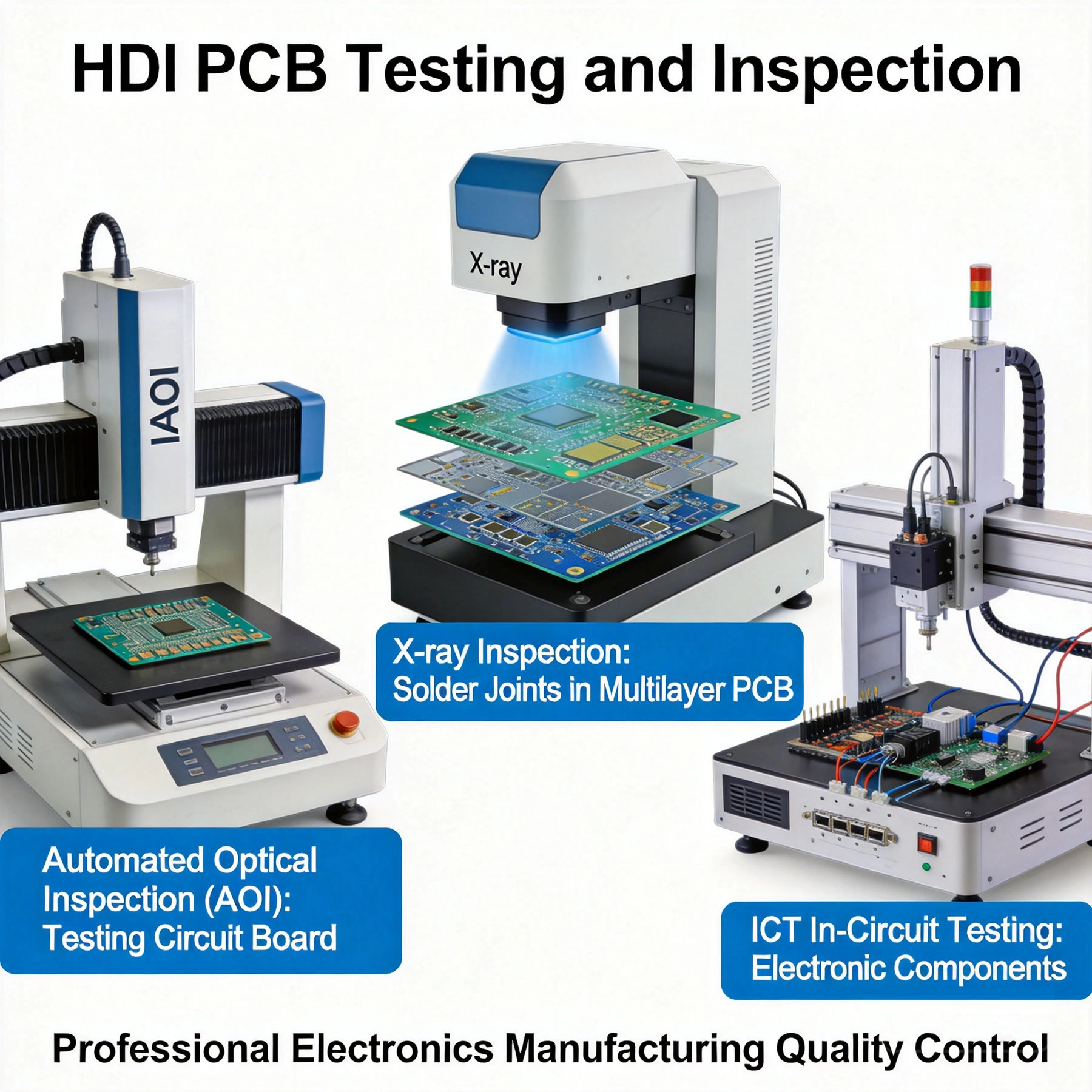
Advanced Testing Methods for High-Density Interconnect PCBsMay/28/2026Testing high-density interconnect (HDI) PCBs presents unique challenges that traditional PCB testing methods simply cannot address. The microscopic features, buried vias, and ultra-fine pitch components that make HDI technology powerful also make them extraordinarily difficult to inspect and test....
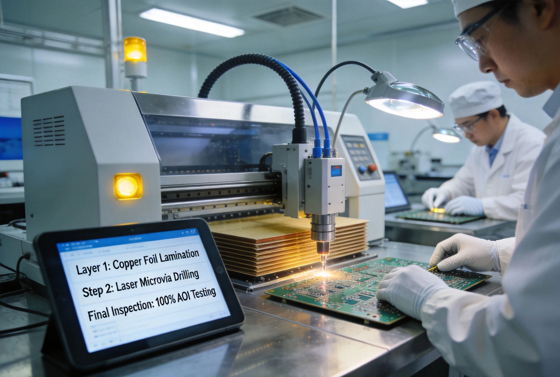
A Step-by-Step Walkthrough of the HDI PCB Manufacturing ProcessMay/28/2026Manufacturing a High Density Interconnect (HDI) PCB is nothing like producing a standard multilayer board. While a regular PCB might go through a dozen steps, an HDI board can require 30 or more distinct operations, each demanding precision equipment and tight process controls. If you've ever wond...