Introduction
When it comes to testing High Density Interconnect (HDI) PCBs, the stakes are higher than ever. These advanced circuit boards feature ultra-fine traces, micro-vias, and component densities that push the boundaries of traditional testing methodologies. Choosing the right testing approach can mean the difference between catching defects early and shipping faulty products to customers.
Flying probe testing and fixture testing represent two fundamental approaches to PCB quality verification. Each method has distinct strengths, limitations, and ideal use cases. For Hdi Boards specifically, the choice becomes even more critical due to their unique construction and accessibility challenges.
This comprehensive comparison will help you understand which testing methodology best suits your Hdi Pcb requirements, whether you're working with consumer electronics, medical devices, aerospace systems, or any application where reliability is paramount.

Understanding HDI PCB Testing Challenges
Before diving into the comparison, it's essential to understand why Hdi Pcb testing presents unique challenges compared to standard circuit boards.
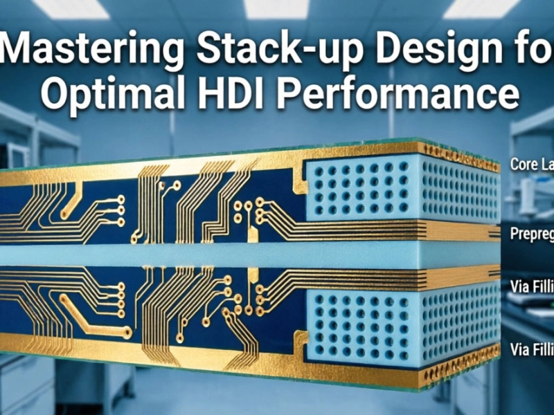
What Makes HDI Boards Different
HDI PCBs are characterized by:
-
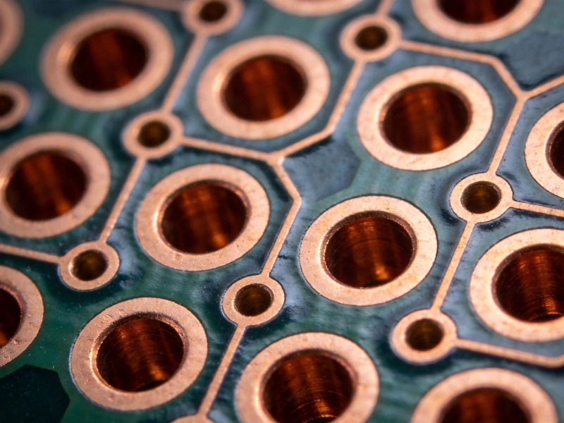
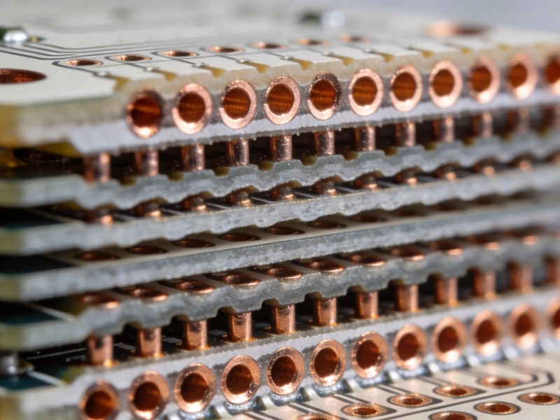
Micro-vias: Vias as small as 50-100 microns in diameter
-
Fine traces: Line widths and spacings of 50 microns or less
-
High layer counts: Often 8-20+ layers in modern applications
-
Blind and Buried Vias: Internal connections not physically accessible
-
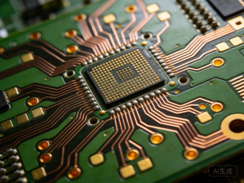
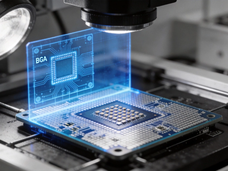
High component density: BGA, QFN, and CSP packages with fine pitch
-
Advanced substrates: High-Tg materials, flex circuits, and rigid-flex combinations
These characteristics create significant testing challenges, as many traditional test access points simply don't exist on Hdi Boards.
What is Flying Probe Testing?
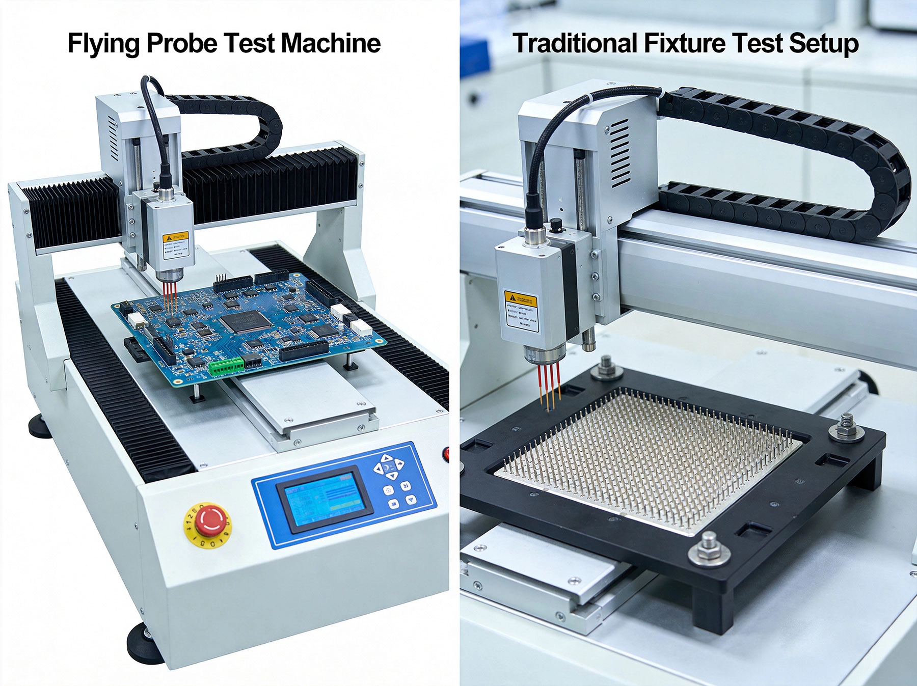
Flying probe testing uses computer-controlled probe heads that "fly" across the board surface, making electrical contact with test points as needed. Unlike traditional fixtures, there's no fixed bed-of-nails array.
How Flying Probe Technology Works
The flying probe system consists of:
-
Multi-axis positioning system: Precisely moves probes to any location on the board
-
Spring-loaded probe tips: Make temporary contact with test points
-
High-speed switching: Routes connections between probes and test instrumentation
-
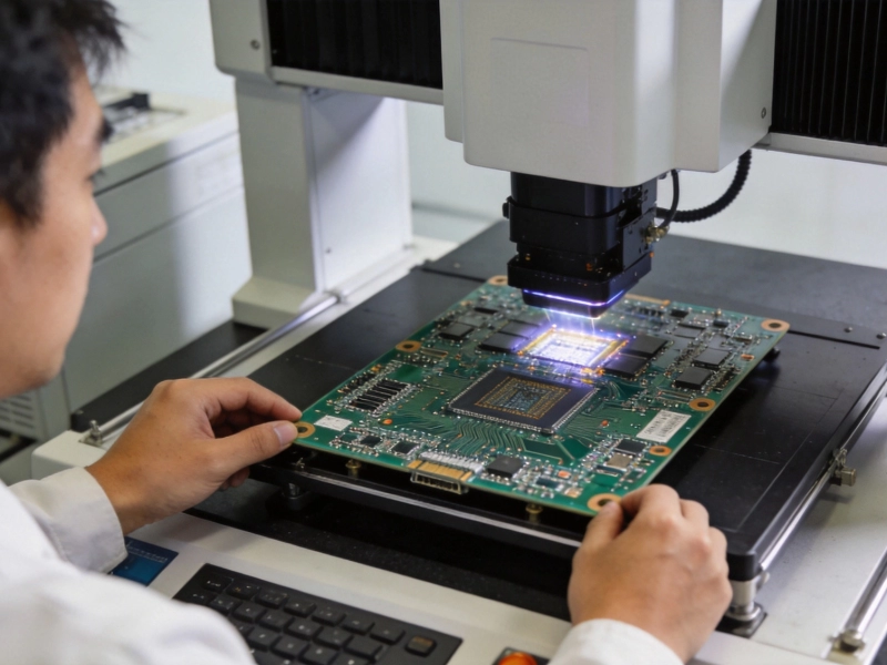
Vision systems: Align probes with fiducial marks and test points
-
Software control: Executes test programs with flexibility and precision
Advantages of Flying Probe for HDI
-
No fixture cost: Eliminates expensive custom fixture fabrication
-
Unlimited test points: Can access any visible pad or via
-
Rapid program changes: Ideal for prototypes and small batches
-
Non-destructive Testing: Gentle probing won't damage fine features
-
Fine pitch accessibility: Probes can reach 100-micron test points
-
Boundary Scan compatibility: Works seamlessly with JTAG and other protocols
Limitations of Flying Probe
-
Longer test times: Sequential probing is slower than parallel fixture testing
-
Limited to visible points: Cannot directly test buried nodes
-
Lower test coverage: May miss some defects detectable by fixtures
-
Power delivery challenges: Injecting current through probes has limits
What is Fixture Testing?
Fixture testing, often called "bed of nails" testing, uses a custom-manufactured fixture with hundreds of spring-loaded pins that simultaneously contact all test points on the board.
How Fixture Technology Works
Traditional fixture test systems include:
-
Fixture frame: Rigid structure holding the nail array
-
Spring-loaded pins: Hundreds to thousands of contacts
-
Wire harness: Connects pins to test instrumentation
-
Pneumatic actuation: Raises and lowers the fixture
-
Test adapter electronics: Switches and routing between UUT and instruments
Advantages of Fixture Testing for HDI
-
Parallel testing: All points tested simultaneously for speed
-
High throughput: Ideal for high-volume production
-
Complete coverage: Extensive node access with dedicated probes
-
Power injection: Can drive higher currents for functional tests
-
Built-in testability: Designs can incorporate testability features
-
Mature technology: Well-understood and widely supported
Limitations of Fixture Testing
-
Fixture cost: Custom fixtures can cost $5,000-$50,000+
-
Long lead times: Fixture fabrication takes weeks
-
Design constraints: Test points must be placed for fixture access
-
Minimum pitch limits: Fixture pins typically require 400+ micron pitch
-
Board size limitations: Large boards require proportionally large fixtures
-
Rework for design changes: Any board revision requires fixture updates
Head-to-Head Comparison for HDI Applications
Test Coverage
For HDI PCBs, test coverage becomes a critical consideration:
|
Test Aspect
|
Flying Probe
|
Fixture
|
|
Visible test points
|
Excellent - any accessible point
|
Good - requires design planning
|
|
Buried node access
|
Limited - relies on Boundary Scan
|
Good - with dedicated test structures
|
|
Fine pitch capability
|
Superior - down to 100 microns
|
Limited - typically 400+ microns
|
|
High-frequency testing
|
Good - short probe leads
|
Excellent - optimized fixtures
|
Cost Considerations
The cost comparison between methods varies significantly based on volume:
-
Prototype/low volume (<100 boards): Flying probe dramatically cheaper - no fixture investment
-
Medium volume (100-1,000 boards): Flying probe still cost-effective; fixture amortized over more units
-
High volume (>1,000 boards): Fixture becomes more economical due to speed advantages
-
Very high volume (>10,000 boards): Fixture essential for production throughput
Time to Market
In today's fast-paced development environment:
-
Flying probe: Test programs ready in days; instant changes for revisions
-
Fixture: 2-4 weeks for fabrication; significant lead time for changes
For HDI PCB products with frequent design iterations, flying probe offers significant time-to-market advantages.
Which Testing Method Should You Choose?
Choose Flying Probe When:
-
Developing prototypes or pre-production samples
-
Producing low to medium volumes (under 1,000 units)
-
Working with ultra-fine pitch HDI features
-
Needing rapid test program development
-
Testing frequent design revisions
-
Budget is limited for custom fixtures
-
Testing large or irregularly shaped boards
-
Working with flex or rigid-flex circuits
Choose Fixture Testing When:
-
Producing high volumes (thousands of units)
-
Requiring maximum test throughput
-
Needing very high current injection capability
-
Performing functional or burn-in testing
-
Board design allows dedicated test points
-
Long-term product lifecycle with stable designs
-
Requiring consistent, repeatable test routines
The Hybrid Approach for HDI
Many manufacturers are discovering that the optimal strategy involves combining both testing methods.
Strategic Test Flow
-
Prototype stage: Flying probe for rapid verification and design validation
-
Pre-production: Flying probe for qualification testing
-
Production ramp: Fixture implementation while maintaining flying probe for revisions
-
Volume production: Fixture for primary testing; flying probe forspot checks and failure analysis
Benefits of the Hybrid Model
-
Best of both worlds - speed and flexibility
-
Reduced risk during fixture development
-
Faster ramp-up for new products
-
Backup testing capability
-
Comprehensive failure analysis resources
Best Practices for HDI Test Implementation
Design for Testability (DFT)
Regardless of your chosen method, DFT principles improve test coverage:
-
Include test access points (TAPs) for internal nodes
-
Provide adequate clearance around test points
-
Design probe targets of sufficient size (0.5mm minimum)
-
Consider boundary scan (JTAG) for inaccessible nodes
-
Include known-good test structures on panel coupons
Communication with Your CM
Effective testing requires partnership with your contract manufacturer:
-
Share test requirements early in the process
-
Discuss test point accessibility during design review
-
Understand their testing capabilities and limitations
-
Establish test coverage targets and acceptance criteria
-
Review test data and defect trends regularly
Emerging Trends in HDI Testing
The testing landscape continues evolving with new technologies:
-
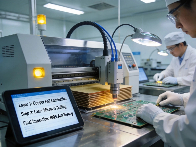
Automated Optical Inspection (AOI) integration: Combined visual and electrical testing
-
AI-powered defect detection: Machine learning for improved fault coverage
-
Non-contact testing: Capacitive and inductive sensing methods
-
In-system programming: Testing and programming in a single fixture
-
Real-time statistical process control: Continuous monitoring of test data
Conclusion
Choosing between flying probe vs. fixture testing for HDI PCBs isn't a one-size-fits-all decision. The right choice depends on your specific product requirements, production volumes, and business priorities.
For prototype development, low-volume production, or products with frequent design changes, flying probe testing offers unmatched flexibility and cost efficiency. Its ability to access ultra-fine pitch features makes it particularly valuable for modern HDI boards.
For high-volume production where throughput is paramount, traditional fixture testing delivers the speed and consistency needed to maintain profitable manufacturing operations.
The most successful approach often combines both methods, leveraging each technology's strengths while mitigating their individual limitations. By understanding the trade-offs and planning your testing strategy early in the design phase, you can achieve optimal quality, cost, and time-to-market outcomes for your HDI PCB products.