
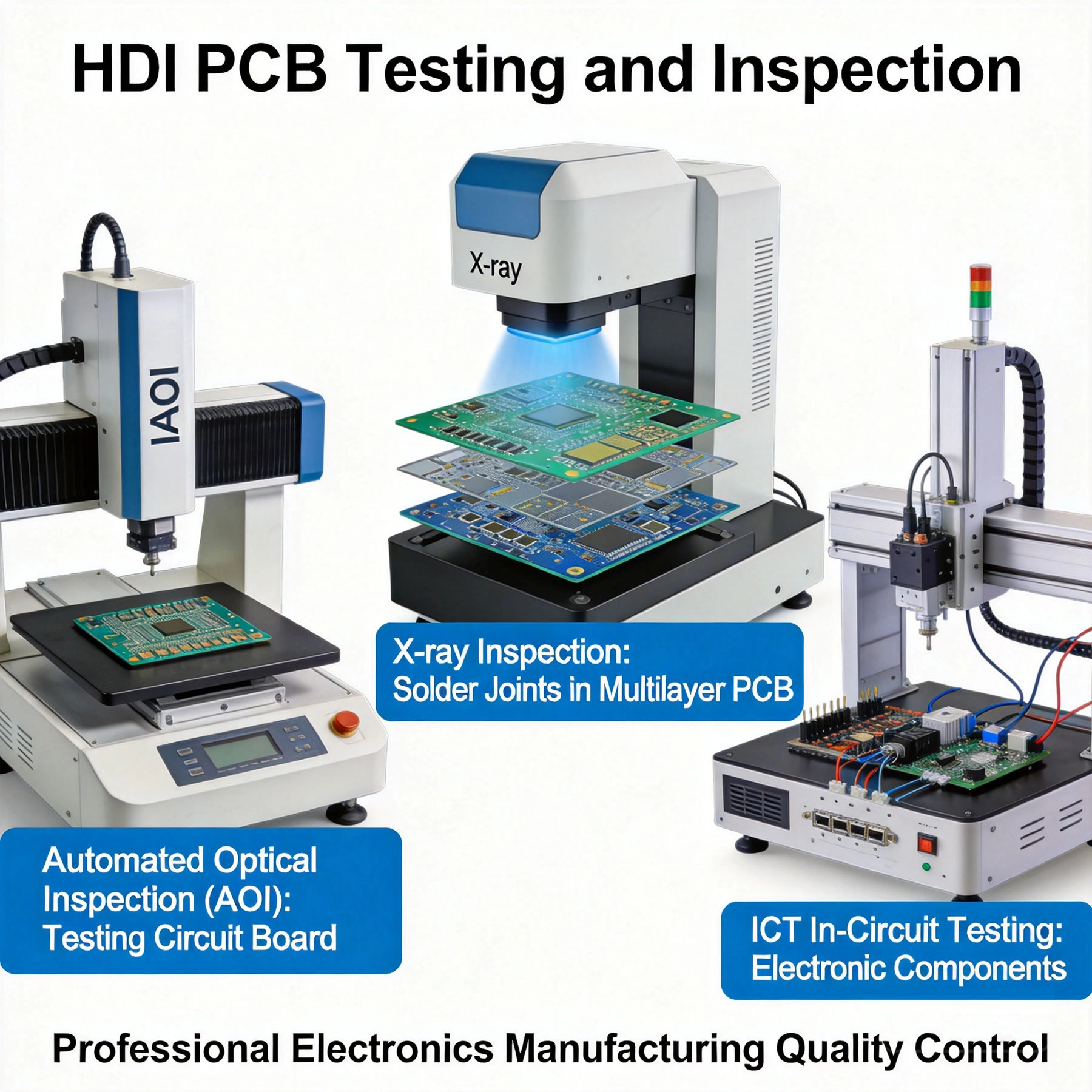
Testing high-density interconnect (HDI) PCBs presents unique challenges that traditional PCB testing methods simply cannot address. The microscopic features, buried vias, and ultra-fine pitch components that make HDI technology powerful also make t...
https://www.high-density-interconnect-pcb.comhttps://www.high-density-interconnect-pcb.com/hdi-pcb-design-testing/advanced-testing-methods-for-high-density-interconnect-pcbs/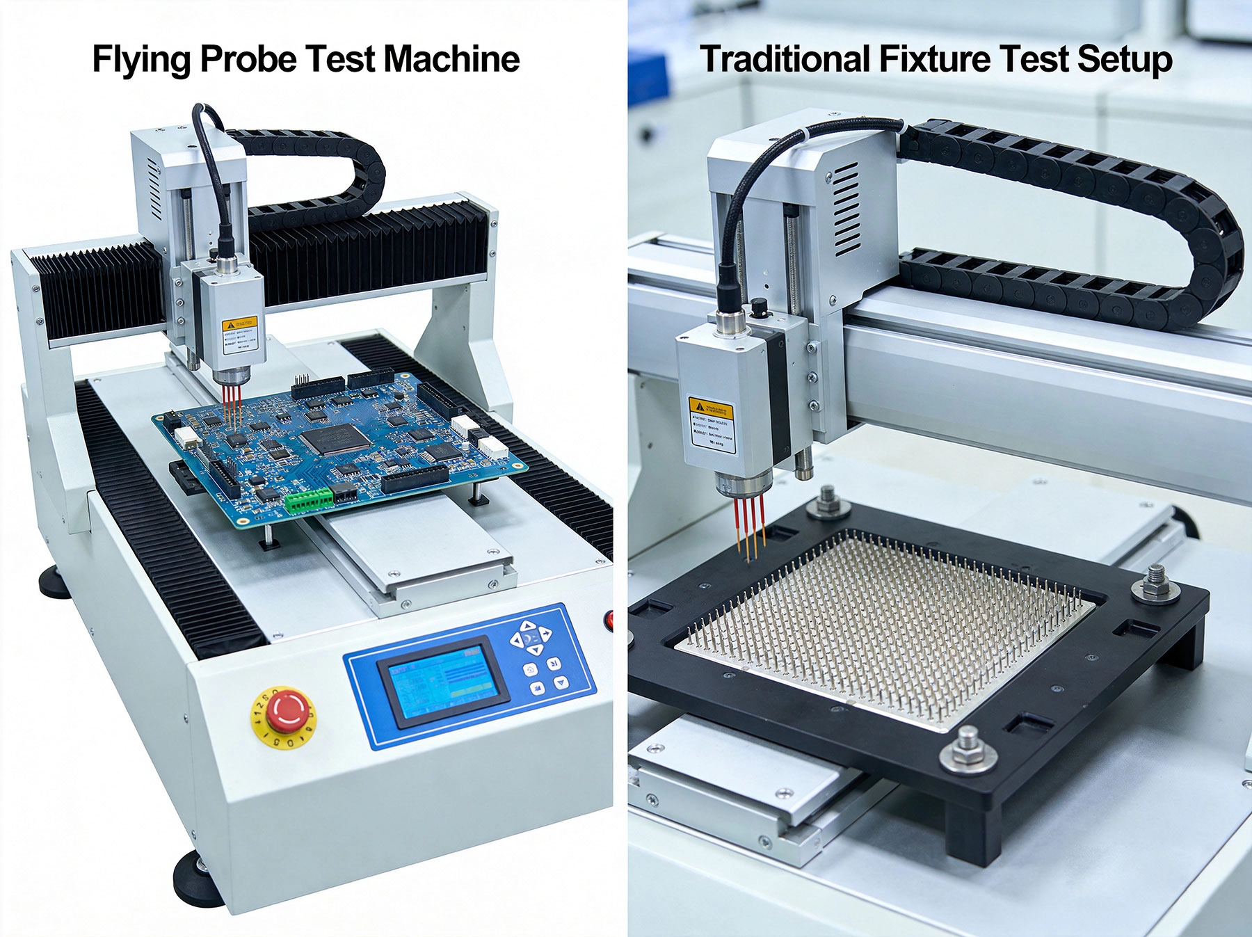
Introduction When it comes to testing High Density Interconnect (HDI) PCBs, the stakes are higher than ever. These advanced circuit boards feature ultra-fine traces, micro-vias, and component densities that push the boundaries of traditional tes...
https://www.high-density-interconnect-pcb.comhttps://www.high-density-interconnect-pcb.com/hdi-pcb-design-testing/flying-probe-vs-fixture-testing-which-is-best-for-hdi-pcbs/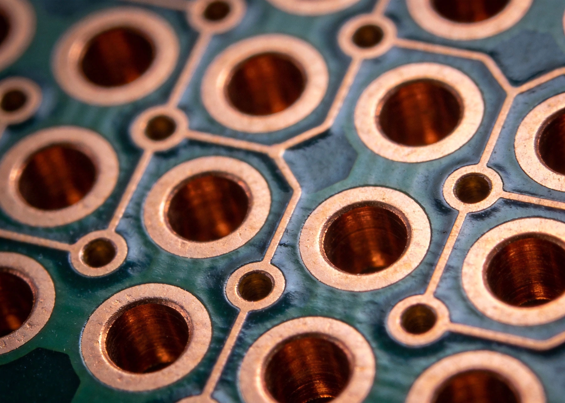
As PCB technology advances and device geometries shrink, the humble via—the plated hole that connects layers in a printed circuit board—has become one of the most critical and most vulnerable elements in modern electronics. Microvias, defined by th...
https://www.high-density-interconnect-pcb.comhttps://www.high-density-interconnect-pcb.com/hdi-pcb-design-testing/the-importance-of-electrical-testing-for-microvia-reliability/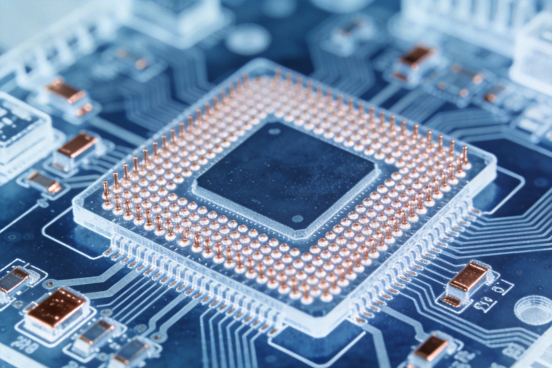
The semiconductor industry keeps shrinking feature sizes while packing more functionality into each chip. The result: Ball Grid Array packages with pitches of 0.4mm, 0.3mm, and even 0.2mm, mounted on HDI substrates that route signals through microv...
https://www.high-density-interconnect-pcb.comhttps://www.high-density-interconnect-pcb.com/hdi-pcb-design-testing/overcoming-the-challenges-of-testing-fine-pitch-bga-on-hdi/