
High Density Interconnect (HDI) boards enable the Miniaturization and performance requirements of modern electronics, but these benefits come with increased complexity in Impedance Control. As trace widths decrease, layer counts increase, and feature density rises, maintaining impedance within specified tolerances becomes increasingly challenging. Impedance mismatches create Signal Integrity problems that manifest as reflections, timing errors, and data corruption in high-speed digital systems and signal loss in RF applications. Understanding how to measure and control impedance tolerance enables engineers to achieve reliable signal performance in even the most demanding Hdi Applications.
Impedance matching between transmission lines, drivers, and receivers ensures maximum power transfer and minimum signal reflection in high-speed circuits. When impedance varies from the specified value, signal reflections occur at discontinuities, creating distortion that degrades Signal Integrity. For digital systems, these reflections cause timing errors, eye diagram closure, and increased bit error rates. For RF systems, impedance mismatches cause return loss, standing waves, and reduced power transfer efficiency.
HDI designs amplify Impedance Control challenges through several mechanisms. Smaller trace widths increase sensitivity to dimensional variations from etching tolerances. More layers increase the number of reference planes and the complexity of layer interactions. Microvias and Blind Vias create discontinuities that require careful impedance management. The combination of these factors means that design techniques that work adequately for standard boards often prove insufficient for HDI designs.
Characteristic impedance defines the relationship between voltage and current on a transmission line. For a lossless line, impedance depends only on the line geometry and the dielectric constant of the surrounding material. The characteristic impedance equals the square root of inductance per unit length divided by capacitance per unit length. This relationship means that any factor affecting inductance or capacitance affects impedance.
Most high-speed designs target 50-ohm single-ended impedance and 100-ohm differential impedance, though other values exist for specific applications. The impedance tolerance specification determines the acceptable variation from the target value. Standard applications typically accept plus or minus 10 percent tolerance, while high-speed digital and RF applications often require plus or minus 5 percent or tighter tolerances.
Differential impedance depends on both the single-ended impedance of each trace and the coupling between the two traces in the differential pair. Tighter coupling between traces reduces differential impedance, while looser coupling allows each trace to behave more independently. Designers can adjust differential impedance by varying trace spacing, trace width, and the distance to reference planes.
Differential impedance tolerance requirements often exceed single-ended requirements because differential signaling relies on precise matching between the two signal paths. Mismatches between the two traces in a differential pair create common-mode noise and reduce common-mode rejection ratio, degrading signal integrity even when the nominal differential impedance meets specification.
The dielectric constant (Dk) of the PCB material directly influences impedance, with higher Dk values reducing impedance for a given geometry. Material manufacturers specify Dk with tolerances typically ranging from plus or minus 0.02 to plus or minus 0.05, though this variation represents material batch-to-batch differences rather than within-batch uniformity. More importantly, Dk varies with frequency, temperature, and moisture content, creating impedance variations even with consistent geometry.
HDI designs using thinner dielectric layers become more sensitive to Dk variations because the dielectric thickness represents a larger percentage of overall impedance contribution. When using materials with high Dk tolerance, designers must account for worst-case variations or select materials with tighter specifications. High-frequency materials like Rogers laminates typically offer better Dk stability than standard FR4 materials.
Fabrication tolerances create dimensional variations that directly affect impedance. Etching processes cannot produce exact trace widths—etched traces typically run 0.5 to 1 mil narrower than designed widths due to side etching. This variation becomes more significant for narrow traces where a 1 mil variation represents a larger percentage of the total width. HDI designs with fine-pitch traces are particularly susceptible to these variations.
Dielectric thickness variations from lamination tolerances also affect impedance, especially for stripline configurations where the distance to reference planes directly determines impedance. Core and prepreg thickness tolerances typically range from plus or minus 10 percent to plus or minus 15 percent, creating impedance variations that must be accommodated in design margins.
Copper thickness variations from plating processes affect impedance, particularly for outer layer traces where plating adds thickness after etching. Standard copper foil thickness tolerances range from plus or minus 10 percent to plus or minus 15 percent, while electroplated copper thickness can vary more significantly depending on plating uniformity.
Surface roughness of copper foils introduces additional impedance variations, particularly at high frequencies where current flows primarily near the conductor surface (Skin Effect). Rougher surfaces increase effective resistance and slightly modify impedance due to the altered current distribution. High-frequency materials often specify low-profile copper foils to minimize these effects.
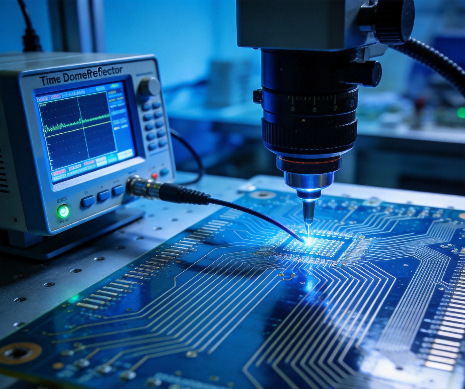
TDR measurement provides the most direct method for characterizing impedance along transmission lines. A TDR instrument launches a fast-rising edge into the transmission line and measures the reflected signal. Reflections from impedance discontinuities return to the instrument at times corresponding to their distance along the line. By analyzing the reflection amplitude and timing, TDR provides impedance profiles along the entire trace length.
Modern TDR systems provide resolution sufficient to detect impedance variations of 1 ohm or better along traces. The measurement bandwidth determines the spatial resolution—higher bandwidth provides better spatial resolution but requires careful calibration to maintain accuracy. For Hdi Boards with short trace segments, high-bandwidth TDR becomes essential to resolve impedance variations that occur over millimeter-scale distances.
Vector network analyzers (VNA) measure impedance in the frequency domain by analyzing reflection coefficients (S11) and transmission characteristics (S21). Frequency domain measurements provide insights into how impedance varies with frequency, which is particularly important for wideband applications where impedance must remain consistent across the operating bandwidth.
VNA measurements require careful calibration to account for test fixtures, cables, and connectors. De-embedding techniques remove the effects of test fixtures, revealing the true characteristics of the device under test. For high-frequency Hdi Applications, frequency domain measurements complement TDR by revealing frequency-dependent impedance behavior that TDR cannot capture.
Impedance test coupons provide standardized structures for measuring impedance on production panels. These coupons include representative transmission line structures designed with the same layer stackup, materials, and processing parameters as the production boards. By measuring impedance on test coupons, manufacturers can verify process capability and control without requiring measurement on every production board.
Effective test coupon design includes multiple impedance structures covering the range of geometries used in production. Single-ended microstrip and stripline structures, differential pairs with various spacing, and structures with different reference plane configurations should all be represented. Test coupon placement should ensure consistent processing with production boards—placing coupons at panel edges may not represent interior board conditions due to processing variations.
Accurate impedance calculation begins with appropriate field solver selection. 2D field solvers provide adequate accuracy for simple geometries where cross-sectional dimensions remain constant along the trace length. For complex geometries with varying reference plane conditions, 3D field solvers provide more accurate results at the cost of increased computation time.
Field solver accuracy depends on accurate material property input. Use material datasheet values for dielectric constant and loss tangent, but account for the frequency dependence of these parameters. Most materials exhibit lower dielectric constants at higher frequencies, and using low-frequency values for high-speed designs will overestimate impedance. Many field solvers include material models that account for this frequency dependence.
DFM practices improve impedance manufacturability by designing within process capabilities rather than pushing limits that create tight tolerance requirements. Use trace widths and dielectric thicknesses that provide adequate impedance margin given fabrication tolerances. When tight tolerances are unavoidable, specify impedance requirements with appropriate acceptance criteria rather than absolute values that cannot be achieved consistently.
Layer stackup design significantly affects impedance control. Symmetric stackups provide more consistent processing and better impedance control than asymmetric stackups. When asymmetry is unavoidable, document the reference plane relationships clearly and work with fabricators to understand the impedance implications.
Clear documentation of impedance requirements prevents misunderstandings between design and manufacturing. Specify impedance requirements including target impedance, tolerance, and measurement method. Provide impedance control data sheets that list the dimensions and material properties used for impedance calculations. When special requirements exist, explain the application requirements that drive the specification.
Communication with fabricators during design review catches potential impedance issues before fabrication begins. Experienced fabricators can review impedance calculations and identify whether the specified tolerances are achievable given their process capabilities. This collaborative approach prevents production delays and ensures realistic expectations.
Manufacturers with proven process capability for impedance control deliver consistent results that meet tight tolerance requirements. Process capability indices (Cpk) above 1.33 indicate that the process consistently produces results within specified tolerances. Ask potential fabricators for process capability data demonstrating their ability to meet your impedance requirements.
Statistical process control (SPC) monitors impedance measurements from test coupons to detect process drift before it creates out-of-tolerance results. Control charts tracking impedance measurements over time reveal trends that indicate process changes requiring intervention. SPC transforms impedance control from reactive correction to proactive prevention.
Consistent material characteristics provide the foundation for impedance control. Use materials from the same manufacturer and batch for critical production runs when possible. When material changes are necessary, verify that the new material properties fall within acceptable ranges and adjust impedance calculations accordingly.
Material handling practices affect dielectric properties, particularly moisture absorption. Store materials in controlled humidity environments and follow recommended bake-out procedures before lamination. Moisture absorbed into dielectric materials changes the dielectric constant and creates impedance variations that can exceed specified tolerances.
Etching parameters significantly affect trace dimensions and therefore impedance. Etch rate, etchant concentration, and temperature all influence the final trace width. Optimize these parameters for the specific copper foil type and trace geometries used in your design. Fine-pitch traces may require different etching parameters than wider traces to achieve consistent results.
Lamination parameters affect dielectric thickness and therefore impedance. Pressure, temperature, and dwell time during lamination determine the final dielectric thickness. Consistent lamination processes yield consistent impedance, while process variations create impedance drift that requires compensation in later processing steps.
Establish clear acceptance testing protocols that define impedance measurement methods, sampling plans, and acceptance criteria. Specify whether measurements occur on test coupons or production boards, and define the measurement frequency required for lot acceptance. Clear protocols prevent disputes about whether production meets specifications.
Sampling plans should balance statistical confidence against testing cost. For critical applications, 100 percent impedance testing may be justified. For less critical applications, sampling plans that provide 95 percent confidence with acceptable risk levels reduce testing burden while ensuring Quality Control.
When impedance measurements fall outside specifications, systematic root cause analysis prevents recurrence. Cross-section analysis reveals actual trace dimensions and dielectric thicknesses that can be compared to design values. Material analysis confirms that dielectric properties meet specifications. Process data review identifies processing variations that may have contributed to the failure.
Corrective actions should address root causes rather than symptoms. When dimensional variations cause impedance failures, adjust etching or lamination parameters. When material variations cause problems, implement stricter material control procedures. Document corrective actions and verify effectiveness through subsequent measurements.
What impedance tolerance can I realistically achieve in Hdi Boards?
Realistic impedance tolerance depends on design complexity and fabricator capability. For well-designed boards processed by capable manufacturers, plus or minus 10 percent is generally achievable. Plus or minus 5 percent requires careful design, material selection, and process control. Tolerances tighter than plus or minus 5 percent become increasingly difficult and expensive to achieve consistently.
How do Microvias affect impedance?
Microvias create impedance discontinuities that require careful design. The absence of a continuous reference plane at the via location creates inductance that affects impedance. Design strategies include providing ground vias adjacent to signal vias to maintain return path continuity, keeping via lengths minimal, and using back-drilling or Buried Via structures that minimize discontinuities.
Should I specify impedance in ohms or as a dimension?
Specifying impedance in ohms with appropriate tolerance is the standard approach that communicates the electrical requirement directly. However, providing the calculated dimensions used to achieve that impedance helps fabricators understand the design intent. Some manufacturers prefer dimensional specifications because they directly control those dimensions, but impedance specifications better represent the actual requirement.
How does dielectric constant variation with frequency affect impedance?
Dielectric constants typically decrease at higher frequencies, causing impedance to increase. The effect magnitude depends on material characteristics—some materials exhibit more significant variation than others. For applications with wide bandwidth requirements, calculate impedance at the highest operating frequency and verify that the resulting value remains within tolerance across the entire bandwidth.
Can I measure impedance on assembled boards?
Measuring impedance on assembled boards presents challenges because components and solder joints introduce discontinuities. TDR measurements can still provide useful information by isolating transmission line sections that remain accessible, but the presence of components complicates interpretation. For complete impedance verification, measurements on bare boards or test coupons provide more accurate results.
Impedance control in HDI boards requires coordinated effort across design, material selection, manufacturing, and testing phases. Understanding the factors that affect impedance enables engineers to design boards that can be manufactured within required tolerances. Selecting appropriate materials with stable dielectric properties, designing within process capabilities, and communicating requirements clearly to fabricators all contribute to achieving impedance targets.
Measurement techniques like TDR and frequency domain analysis provide the data needed to verify impedance performance and identify problems before boards reach production. When combined with statistical process control in manufacturing, these measurement tools transform impedance control from guesswork into disciplined engineering.
Approach impedance control as a system-level challenge rather than a series of isolated parameters. The interactions between dielectric properties, dimensional variations, and process parameters create complex behaviors that require holistic understanding. When designers, fabricators, and test engineers collaborate with shared understanding of impedance requirements, HDI boards deliver the performance that modern high-speed and RF applications demand.
How to Read and Interpret HDI PCB Stack-up Drawings?July/14/2026
An Introduction to Microvia Technology in HDI PCBsJuly/24/2026
Troubleshooting Common Issues in HDI PCB AssemblySeptember/09/2026

Implementing a Robust Quality Control System for HDI ManufacturingJune/15/2026
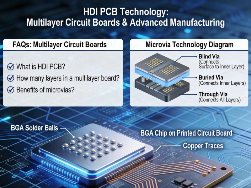
Top 10 Frequently Asked Questions About HDI PCB TechnologyMay/28/2026
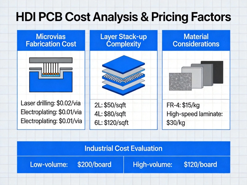
HDI PCB Cost Guide: What Factors Drive the Price Up?June/16/2026
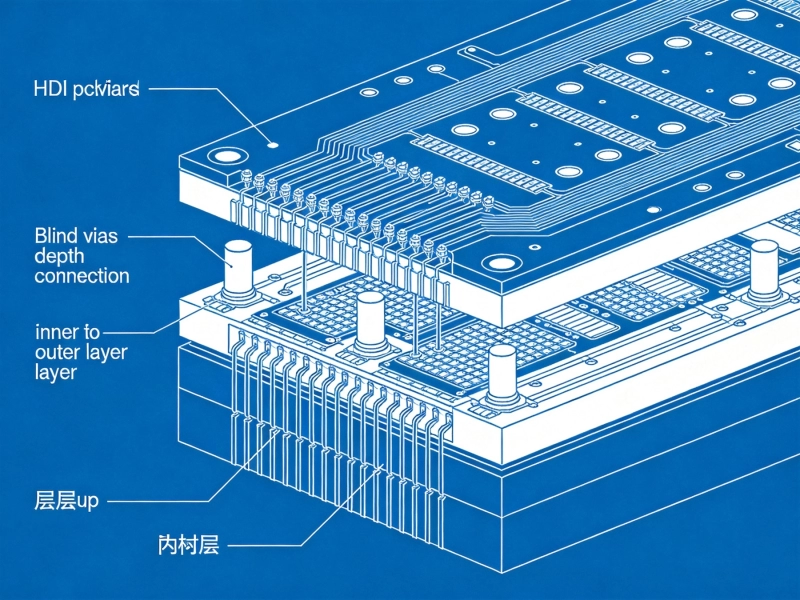
Understanding HDI Terminology: A Glossary for EngineersAugust/03/2026
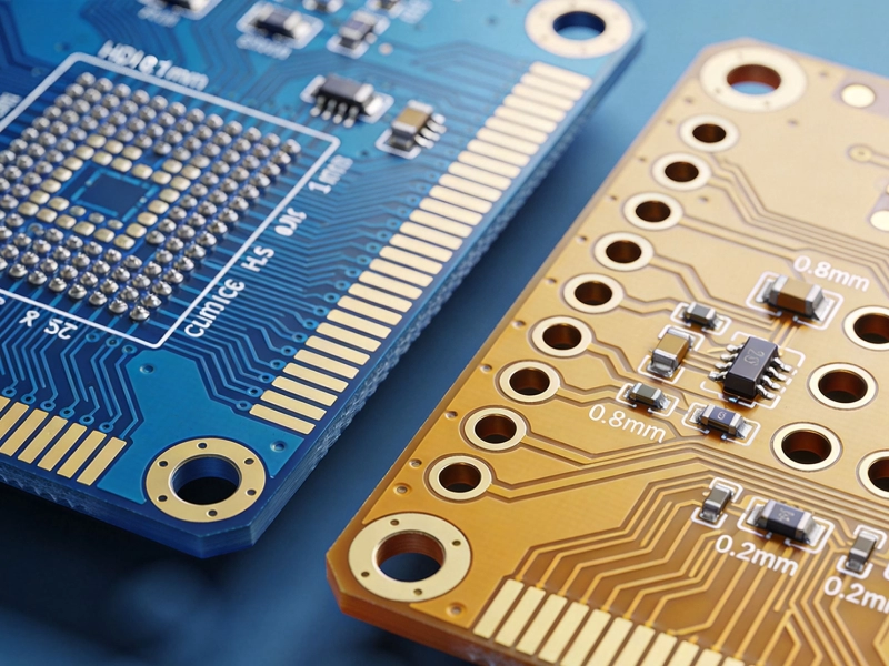
Understanding the Core Differences Between HDI and Traditional PCBsJuly/02/2026