Open Nav

High Density Interconnect (HDI) printed circuit boards have become indispensable in modern electronics, powering everything from smartphones to medical devices. At the core of Hdi Technology lie Microvias—tiny structures that enable unprecedented routing density. Yet despite their small size, Microvias present some of the most demanding manufacturing challenges in the PCB industry. Plating and filling these microscopic features reliably and consistently separates capable HDI manufacturers from those still struggling with basic capability. Understanding these challenges helps designers make informed decisions that balance performance requirements against manufacturing reality.
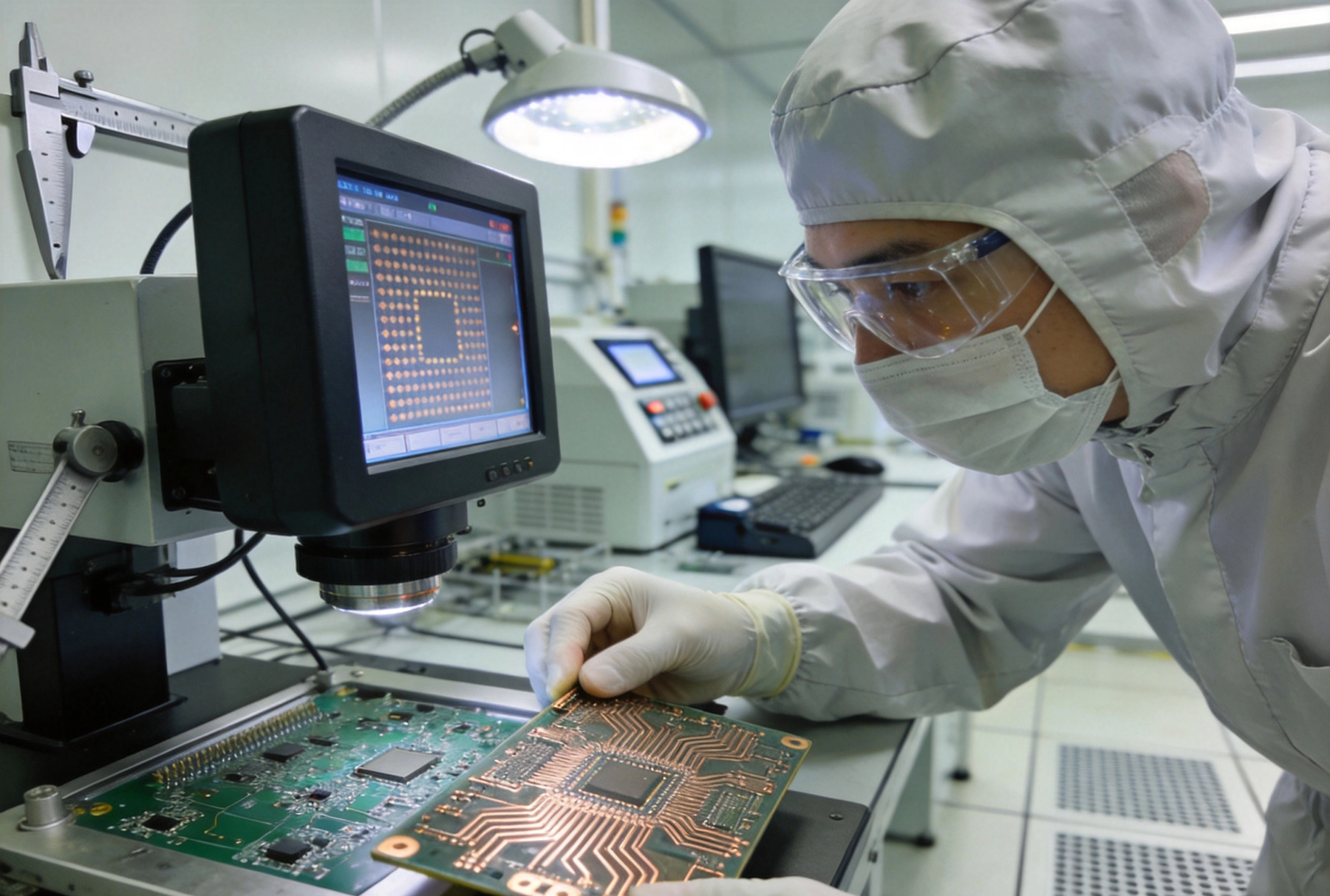
Unlike larger through-hole vias that can be drilled and plated with relatively forgiving tolerances, microvias require sub-50-micron precision throughout their formation and metallization. The copper plating inside a Microvia must achieve uniform thickness despite the geometry's inherent challenges—a high aspect ratio barrel with small diameter creates flow patterns that resist uniform current distribution during electroplating. Variations in plating thickness compromise reliability, as thin spots become failure points under thermal stress or mechanical vibration.
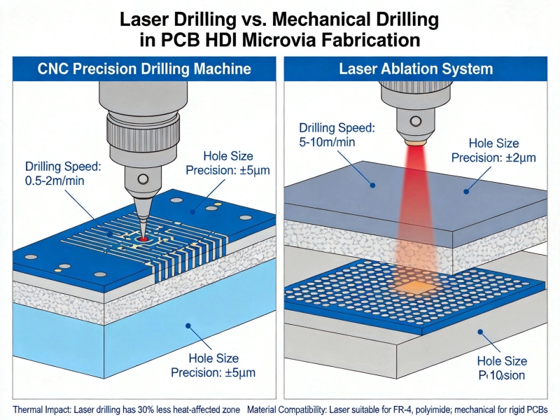
The catalytic activation process preceding copper plating presents additional complexity. Hdi Boards typically use laser ablation to form microvias, which leaves carbonized residue along the via walls that inhibits proper plating adhesion. Desmear processes remove this residue but must be carefully controlled—over-processing damages surrounding Dielectric Material while under-processing leaves contamination that causes voiding or delamination. This cleaning step often determines whether subsequent plating will achieve the void-free uniformity that Hdi Reliability demands.
Copper grain structure within the plated metal significantly impacts Microvia performance. Plating parameters including current density, solution flow rate, and additive concentrations influence grain orientation and size, which in turn affect ductility, conductivity, and stress resistance. Fine-grained copper with consistent orientation provides superior fatigue resistance for applications involving thermal cycling, while coarser grain structures may suffice for more benign environments. Advanced manufacturers monitor grain structure through cross-section analysis and adjust plating chemistries to optimize for specific application requirements.
Microvia filling serves multiple purposes depending on the application. In blind and Buried Vias intended for electrical interconnection, filling may be unnecessary beyond the structural plating—though even here, complete void-free plating remains essential. For Thermal Vias carrying heat away from power components, conductive or non-conductive fills dramatically improve Thermal Performance. Invia-in-pad configurations, fills prevent solder from wicking away during assembly, ensuring reliable solder joints.
The physical scale of microvias creates filling challenges unknown in Traditional Pcb processing. Capillary forces dominate fluid behavior at small scales, drawing filling materials into tight spaces while trapping air pockets that form voids. Surface tension effects that are negligible in larger structures become primary concerns for 50-100 micron features. These physics explain why filling processes that work reliably for 300-micron vias often fail catastrophically for their smaller cousins.
Multiple filling approaches have evolved to address different requirements. Each method involves trade-offs between cost, process complexity, and achieved fill quality. Selection depends on the specific application, production volume, and reliability requirements. Understanding these trade-offs helps designers specify requirements that manufacturing can meet consistently rather than aspirational targets that compromise yield and increase cost.
Conductive filling uses copper or silver-filled epoxies to completely fill the microvia barrel after initial plating. Copper paste filling provides excellent thermal and electrical conductivity, making it ideal for Thermal Vias and high-current applications. The process begins after desmear and first-plate copper, applying conductive paste through stenciling or screening that forces material into via barrels. Multiple applications may be necessary for deeper features, with intermediate curing steps between passes.
The challenge with conductive pastes lies in achieving void-free filling while maintaining precise volume control. Paste rheology—its flow characteristics—must balance between filling capability and tendency to squeeze out of vias during application. Additives that improve filling can cause paste to migrate onto pad surfaces where it creates contamination. Successful conductive filling requires precisely controlled paste formulations matched to specific via geometries, often developed through extensive trial and error with each new stackup configuration.
Silver-filled epoxies offer even higher conductivity than copper pastes but introduce compatibility concerns. Silver migration under bias voltage can create short circuits over time, limiting use in high-voltage or moisture-prone environments. Silver also costs more than copper, making silver-filled approaches premium options reserved for applications where conductivity differences provide meaningful performance benefits. Many designs achieve adequate Thermal Performance with copper paste, reserving silver for specialized applications where the additional conductivity justifies cost and migration risks.
Non-conductive fills use dielectric polymers to plug microvias, preventing solder wicking without providing thermal or electrical conductivity through the fill. This approach costs less than conductive filling and avoids migration concerns, making it the default choice for many Via-in-pad applications where conductivity is unnecessary. Non-conductive fills also enable smaller capture pad sizes by eliminating concerns about conductive paste spreading between adjacent features.
Acrylic and epoxy-based fills represent the most common non-conductive approaches, each offering different property trade-offs. Acrylic systems cure quickly and provide good flexibility but may not withstand extreme thermal cycling. Epoxies offer superior thermal resistance and chemical stability but require longer cure cycles that impact throughput. Fill material selection should consider the expected service environment, with more demanding applications favoring materials proven through extended thermal cycling testing.
Void formation in non-conductive fills often traces to air entrapment during application or outgassing from underlying materials during curing. Vacuum-assisted filling addresses air entrapment by applying pressure before application and maintaining vacuum during filling. Controlling outgassing requires understanding the thermal history of the board—materials that have seen multiple lamination cycles may release trapped volatiles at unexpected points in subsequent processing. Qualified filling processes account for these factors through validated parameter sets developed through systematic experimentation.
Via capping creates a conductive or dielectric cap over the plated through-hole without completely filling the barrel. This approach provides some solder flow protection while avoiding the complexity of full filling processes. Capped vias maintain the original plated barrel, preserving its electrical and thermal properties while preventing solder from entering the via cavity. For thermal vias where conductivity through the barrel matters, capping preserves the thermal path that filling would interrupt.
Copper capping electrolytically deposits additional copper over the via mouth, creating a planar surface flush with surrounding copper. This approach maintains excellent thermal and electrical conductivity through the barrel while eliminating solder wicking concerns. The process requires careful control to avoid overplating that creates surface irregularities or underplating that leaves depressions where contamination accumulates. Multiple thin plating steps typically produce better results than single thick applications.
Conductive paste capping uses small amounts of conductive material to bridge the via opening, achieving similar results to copper capping at potentially lower cost. The challenge lies in controlling paste volume precisely—too little leaves gaps while too much creates excess that must be removed. Automated paste application with optical verification addresses these concerns in high-volume production but adds process complexity that increases per-board cost.
Voids represent the most common quality issue in microvia filling, occurring when air or gas pockets become trapped within the filled structure. Voids weaken the fill mechanically and can cause crack propagation under thermal or mechanical stress. In thermal applications, voids reduce effective cross-sectional area for heat transfer, degrading thermal performance below design expectations. Detecting and preventing voids requires understanding their root causes and implementing appropriate controls.
Process parameters most directly influence void formation. Filling speed affects air entrapment—faster application pressures more material into vias before air can escape, trapping bubbles. Temperature influences viscosity and surface tension, with warmer materials generally filling more readily but requiring careful temperature control to maintain consistency. Vacuum levels during application determine how effectively trapped air can be evacuated. Optimizing these parameters for specific via geometries requires systematic experimentation and statistical process control.
Detection methods range from destructive cross-section analysis to non-destructive X-ray Inspection. Cross-sections provide definitive void content information but destroy the inspected sample, limiting use to qualification and periodic sampling. X-ray Inspection can examine 100% of production boards without damage, though image interpretation requires expertise to distinguish actual voids from normal filling variations. Automated X-ray systems with trained defect detection algorithms enable high-speed inspection suitable for production volumes, though equipment and operation costs are substantial.
Microvia filling materials must maintain compatibility with surrounding Pcb Materials across the entire manufacturing and service lifecycle. Thermal expansion mismatches create stress concentrations at material interfaces that can cause delamination during thermal cycling. Dielectric materials in the board core, prepreg bonding layers, and copper foil all have different expansion coefficients, and the filling material must accommodate these differences without failure.
Moisture absorption creates particular challenges for filling materials. Standard PCB substrates readily absorb atmospheric moisture, and this moisture can migrate into filling materials or collect at interfaces. When boards undergo rapid heating during assembly reflow, trapped moisture expands violently, potentially causing delamination or cracking. Proper pre-baking before assembly prevents moisture-related failures but requires additional process steps and added cost. Filling materials with lower moisture absorption reduce this risk but may sacrifice other properties.
Chemical compatibility with assembly processes must also be verified. Flux residues, cleaning solutions, and conformal coatings can interact with filling materials in unexpected ways. Some filling formulations resist common cleaning solvents while others may swell or degrade upon exposure. Understanding the entire production and service lifecycle—including repair and rework processes—prevents field failures from interactions between filling materials and subsequent processing.
Statistical Process Control (SPC) forms the foundation of consistent microvia filling quality. Rather than inspecting finished boards and rejecting defectives, SPC monitors process parameters that determine quality, adjusting before out-of-spec conditions occur. Critical parameters for microvia filling include filling pressure or speed, material temperature and viscosity, vacuum levels, and curing time and temperature. Each parameter has acceptable ranges established through qualification testing and must be maintained within those ranges.
Process capability indices (Cpk) quantify how well a process performs relative to specification limits. Cpk values greater than 1.0 indicate that process variation fits within specification limits, while values greater than 1.33 demonstrate robust processes with meaningful margin. HDI manufacturers capable of microvia filling with Cpk values consistently above 1.33 provide the most reliable partners for demanding applications. Lower capability may be acceptable for less critical applications but increases the probability of field failures.
Incoming material verification ensures that filling materials meet specifications before use. Lot-to-lot variations in fill material properties can shift process performance even when parameters remain constant. Viscosity, filler content, and shelf life all affect filling behavior and must be verified against certificate of compliance data. Materials approaching expiration should be tested before use in critical applications, as aged materials may not perform consistently with fresh lots.
Delamination between fill material and via walls represents a primary failure mode for filled microvias. This separation creates electrical discontinuity or thermal resistance far exceeding design intent. Contributing factors include surface contamination preventing proper adhesion, inadequate curing leaving material in a semi-solid state, and thermal shock exceeding the bond strength. Prevention focuses on process controls that ensure clean surfaces, complete curing, and appropriate thermal handling throughout production.
Cracking in fill material under thermal stress indicates either inadequate material ductility or excessive stress concentrations at geometric transitions. Fill materials must accommodate the differential expansion between copper barrel walls and dielectric contents without cracking. Material selection for specific thermal environments—room temperature only versus automotive thermal cycling, for example—determines whether standard or enhanced formulations are required. Accelerated life testing under representative conditions validates material selection before production commitment.
Solder wicking into unfilled or partially filled vias causes assembly defects including insufficient solder for reliable joints, excessive solder creating bridges, and void formation in solder joints. These defects often escape incoming inspection only to appear during functional test or, worse, in the field. Proper filling to specification with validated process controls prevents wicking defects, though designs that minimize solder exposure to via areas provide additional protection against these failures.
Microvia filling costs scale with process complexity and yield loss rates. Conductive filling commands premium pricing over non-conductive approaches, with silver-filled materials at the high end. Vacuum-assisted filling adds equipment investment and cycle time compared to atmospheric processes. Process selection should match filling requirements to actual application needs rather than over-specifying for margin that provides no functional benefit.
Yield rates significantly impact effective filling cost. Processes with higher inherent void rates may show lower per-board cost but generate more scrap and rework. Total cost accounting includes not just direct filling expense but also inspection, rework, and warranty costs from quality escapes. Manufacturers with mature filling processes typically deliver lower total cost despite higher quoted prices, making capability and track record important selection criteria.
Volume considerations influence process economics as well. Some advanced filling technologies require substantial setup investment that amortizes more favorably at higher volumes. Prototype and low-volume production often use simpler processes with higher per-board cost but lower setup barriers. Design optimization that minimizes required filling—through appropriate via sizing and strategic placement—can shift economics toward simpler processes without sacrificing performance.
Clear communication of filling requirements prevents misunderstandings that compromise quality. Specifications should define not just whether filling is required but also acceptable fill methods, void criteria, and inspection requirements. Ambiguous specifications leave room for manufacturers to interpret intent differently than designers expected, potentially delivering boards that meet the letter of requirements while failing functional needs. Detailed specifications developed collaboratively with manufacturing partners achieve the best outcomes.
Design review with manufacturing partners before layout completion identifies potential filling challenges early. Stackup designs that create aspect ratios or geometries pushing process limits invite quality problems. Early engagement allows designers to adjust layer assignments, via sizes, or component placement to achieve the same electrical and thermal objectives through more manufacturable structures. This collaboration upfront costs little but prevents expensive redesigns later.
Qualification processes validate manufacturing capability for specific designs before committing to production. Qualification boards should represent production worst-case conditions—maximum via count, thinnest dielectrics, most challenging aspect ratios. Comprehensive qualification includes cross-section analysis, thermal cycling testing, and electrical characterization to verify that filled microvias meet all requirements. Short-cut qualification may miss failure modes that appear only under extended stress testing.
Advanced filling materials continue evolving to address current limitations. Lower-viscosity conductive pastes with improved void-free filling represent active development areas, as do materials with better Thermal Conductivity while maintaining processing ease. Nanomaterial additives show promise for enhancing thermal and electrical performance without compromising filling characteristics. These developments may shift process selection criteria as new materials become commercially available.
Alternative formation methods including advanced laser systems and additive copper deposition may eventually supplement or replace traditional filling approaches. Direct metallization of via walls could eliminate filling requirements entirely for many applications. While these technologies remain in earlier development stages, monitoring industry developments helps designers anticipate changes that might simplify manufacturing or enable new performance levels.
Process monitoring and control continue advancing toward real-time quality verification. Inline X-ray systems now provide immediate feedback on filling quality, enabling closed-loop process adjustment rather than end-of-line inspection. Machine learning algorithms analyzing inspection data can identify patterns that predict failures before they occur. These advances promise to improve consistency and reduce cost for high-quality microvia filling.
Plating and filling microvias in HDI production presents genuine manufacturing challenges that demand expertise, equipment, and process discipline. The microscopic scale of these structures amplifies the consequences of minor variations, making precise control essential for consistent quality. Understanding the trade-offs between filling methods—conductive versus non-conductive, vacuum versus atmospheric, copper versus silver—enables informed decisions that balance performance against cost and manufacturing complexity.
Successful microvia filling requires partnership between designers and manufacturers built on clear communication and mutual expertise. Designers who understand filling challenges can create layouts that achieve design objectives through manufacturable structures. Manufacturers who share process knowledge enable designers to optimize for producibility without sacrificing functionality. This collaboration separates successful HDI projects from those plagued by quality issues and cost overruns.
As electronic products continue demanding higher density and performance, Microvia Technology and its associated manufacturing challenges will only grow in importance. Investing in understanding these challenges—whether as a designer specifying requirements or a manufacturer developing capability—builds competitive advantage in an increasingly demanding market. The insights shared here provide a foundation for that investment, though continued learning remains essential as technology evolves.
What causes voids in filled microvias?
Voids form when air or gas becomes trapped during filling or when outgassing from underlying materials creates pockets during curing. Process parameters including filling speed, temperature, and vacuum level directly influence void formation. Surface contamination can also prevent proper material adhesion, creating delamination that appears similar to voids.
How do I choose between conductive and non-conductive microvia filling?
Conductive filling provides thermal and electrical conductivity through the via barrel, making it essential for thermal vias and high-current applications. Non-conductive filling prevents solder wicking without conducting through the barrel, suitable for signal vias and lower-power applications where conductivity is unnecessary. Cost and migration risks favor non-conductive approaches unless conductivity provides meaningful benefit.
What inspection methods detect microvia filling defects?
X-ray inspection provides non-destructive detection of voids, cracks, and fill inconsistencies in production boards. Cross-section analysis offers definitive defect identification but destroys samples, limiting use to qualification and periodic sampling. Automated Optical Inspection can detect surface defects but cannot see inside filled structures.
How does aspect ratio affect microvia filling difficulty?
Higher aspect ratios create longer filling paths that trap air more easily and make complete void-free filling more challenging. Standard processes reliably fill aspect ratios up to 1:1, while deeper vias may require multiple filling steps or alternative approaches. Design optimization that minimizes aspect ratio improves manufacturability.
What thermal testing validates microvia filling reliability?
Thermal cycling testing between temperature extremes appropriate for the application environment validates filled Microvia Reliability. Automotive applications typically require hundreds of cycles from -40°C to +125°C, while consumer electronics may use less demanding profiles. Electrical continuity monitoring during testing identifies intermittent failures, while post-test cross-section analysis reveals damage not apparent during electrical testing.
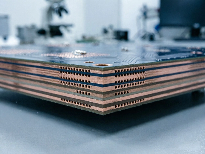
Understanding Sequential Lamination in Multi-Step HDI BoardsJuly/03/2026
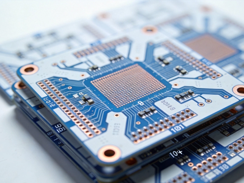
How Manufacturers Achieve High Precision Alignment in 10+ Layer HDI BoardsAugust/15/2026
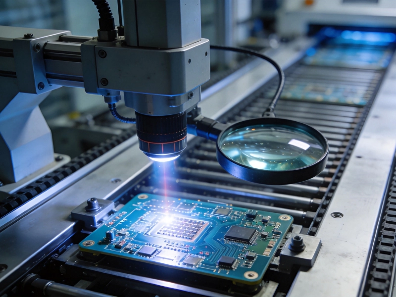
Critical Quality Checkpoints in the HDI Production LineJuly/13/2026
Precision in HDI FabricationJune/04/2026
Overcoming Common Manufacturing Defects in High-Density InterconnectsSeptember/21/2026

What is the Lead Time for Manufacturing Custom HDI Boards?October/12/2026
Challenges of Integrating HDI in High-Efficiency Power InvertersJuly/16/2026
Copper Coin and Embedded Heat Sinks: Advanced Cooling for HDIJuly/08/2026