
High Density Interconnect (HDI) Pcb Technology represents the frontier of electronic manufacturing, enabling designers to pack unprecedented functionality into increasingly compact form factors. From smartphones to aerospace systems, Hdi Boards power the most sophisticated electronics. Yet this advanced capability comes with equally demanding quality requirements. Unlike standard PCBs where defects might be repairable, HDI defects often prove irreparable due to the complexity of Microvia structures and precision fabrication requirements. Understanding and implementing comprehensive quality checkpoints throughout HDI production determines success or failure in this demanding manufacturing domain.
Effective Hdi Quality Control requires systematic inspection at every production stage, with verification points designed to catch problems before they propagate downstream. This comprehensive approach prevents expensive rework, reduces scrap, and ensures that finished boards meet the exacting reliability requirements of modern electronic applications.
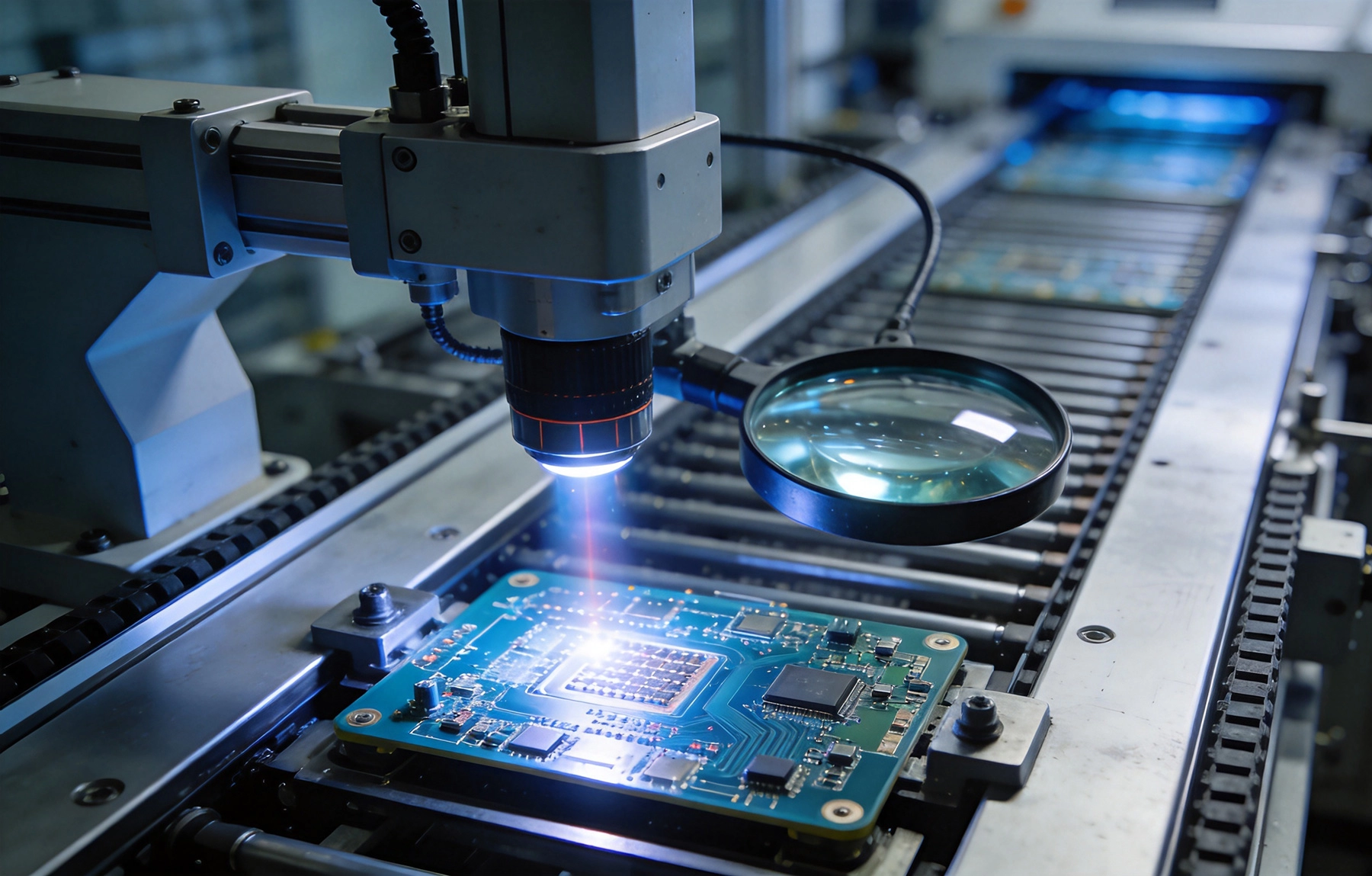
HDI production begins before any processing occurs—with comprehensive material inspection that establishes quality foundations. Materials intended for HDI fabrication must meet exacting specifications for dimensional stability, thermal properties, and laser processing compatibility. Inspection checkpoints include:
Material specifications for Hdi Applications typically exceed requirements for standard PCBs. Dielectric materials must demonstrate higher dimensional stability to maintain Microvia alignment across multiple lamination cycles. Copper foils require lower surface roughness to ensure reliable microvia plating.
Materials stored before HDI fabrication require controlled environmental conditioning to prevent moisture absorption and dimensional changes. Quality checkpoints verify:
Many HDI manufacturers implement material tracking systems that trace individual material lots through entire production runs, enabling root cause analysis if quality problems emerge during fabrication.
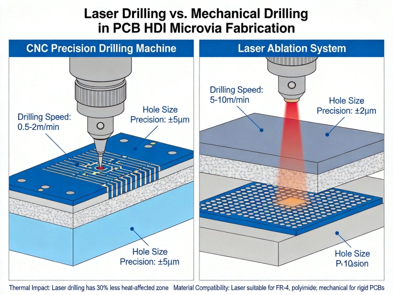
Laser Drilling represents the most critical and challenging process in HDI fabrication. Microvias—typically 75-150μm diameter—must be drilled with extreme precision through multiple dielectric layers while maintaining clean sidewalls and accurate positioning. Quality checkpoints include:
CO2 and UV laser systems each require specific parameter optimization. CO2 lasers excel at drilling through thicker dielectric layers but may produce taper requiring compensation. UV lasers provide finer control for shallow vias but process more slowly. Quality verification must match inspection methods to specific laser system capabilities.
Laser Drilling generates debris—smears, spatter, and residue—that must be completely removed before Copper Plating. Incomplete debris removal causes plating defects and subsequent reliability failures. Inspection checkpoints verify:
Some manufacturers implement in-process AOI (Automated Optical Inspection) immediately after desmear operations, catching debris problems before they affect plating quality.
For plated through-hole vias and filled microvias, Copper Plating quality directly determines electrical reliability. Plated vias must demonstrate complete filling without voids, voids, or plating thickness variations. Quality checkpoints include:
Micro-Xray inspection plays a critical role here, enabling non-destructive examination of internal via structures. Filled microvias require especially rigorous inspection since internal voids cannot be detected through surface examination alone.
Plated vias must demonstrate reliable electrical connections between layers. Electrical testing checkpoints include:
For high-reliability applications like automotive or aerospace, manufacturers often perform accelerated life testing on sample vias, subjecting them to thermal cycling to verify long-term reliability before proceeding with production.
HDI designs feature trace widths and spacings as tight as 75μm or less, requiring precise control during etching and pattern transfer. Quality checkpoints ensure:
Automated optical inspection (AOI) systems perform line-by-line scanning of etched patterns, flagging any features deviating from design specifications. Some systems incorporate adaptive learning that improves detection accuracy over time based on inspection history.
Multilayer Hdi Boards require precise registration between layers, particularly for Stacked Microvias and Buried Vias. Registration checkpoints verify:
Laser Direct Imaging (LDI) systems provide superior registration accuracy compared to traditional photolithography, enabling reliable fabrication of the complex layer stacks that characterize advanced HDI designs.
The multiple lamination cycles required for HDI boards create significant delamination risk. Bonding quality between layers determines long-term reliability. Inspection checkpoints include:
Delamination often manifests during thermal cycling when differing CTEs between materials cause stress. Pre-delivery thermal cycling tests help identify potential delamination risks before boards reach customers.
Multiple lamination cycles cause dimensional changes that must be controlled to maintain precise feature alignment. Dimensional stability checkpoints ensure:
Dimensional stability verification becomes increasingly critical for multi-stage HDI designs where features added in later lamination cycles must align precisely with structures created in earlier cycles.
Solder mask application on HDI boards requires precise control due to fine feature sizes and topographic complexity. Quality checkpoints verify:
For boards with filled microvias, solder mask must properly cover via fills while maintaining proper openings around component pads. This requires careful process control to prevent solder mask intrusion into via structures.
Surface finishes—ENIG, HASL, OSP, or immersion silver—must meet specific criteria for HDI applications. Quality checkpoints include:
Surface finish defects that would be acceptable on standard PCBs—minor thickness variations, slight coverage gaps—become critical on HDI boards where fine features amplify small imperfections.
HDI boards require 100% electrical testing to verify connectivity and isolation across complex interconnect structures. Testing checkpoints include:
Electrical testing for HDI boards often requires specialized test fixtures accommodating fine-pitch features and multiple test points. Flying probe testing systems provide flexibility for prototype and low-volume production, while bed-of-nails fixtures enable efficient testing of higher volumes.
High-reliability applications require comprehensive qualification testing beyond basic electrical verification. Reliability checkpoints include:
For military and aerospace applications, additional testing includes humidity cycling, altitude simulation, and radiation exposure depending on mission requirements.
Hdi Quality Control extends beyond inspection to comprehensive documentation of process parameters. Documentation requirements include:
This documentation enables root cause analysis if quality problems emerge, provides traceability for regulatory requirements, and facilitates process improvement through historical analysis.
Individual material lots and production batches require tracking throughout HDI fabrication. Traceability systems ensure:
Some HDI manufacturers implement RFID tracking for individual boards, enabling detailed production history for each finished assembly. This level of traceability proves essential for high-reliability applications where product failures must be traceable to root causes.
HDI PCB Fabrication demands Quality Control at every production stage, from material inspection through final electrical testing. The complexity of microvia structures, the precision requirements of fine features, and the multiple process cycles required for high-density designs create opportunities for defects that propagate quickly through subsequent operations. Effective quality checkpoint systems prevent these propagation paths, catching problems at the earliest possible stage when corrective action remains practical.
Implementing comprehensive HDI quality controls requires significant investment in inspection equipment, trained personnel, and systematic processes. Yet this investment proves essential for organizations competing in markets where Hdi Technology enables product differentiation. Quality systems designed for HDI fabrication provide the reliability foundation that advanced electronics applications demand.
As Hdi Technology continues advancing—with even smaller features, more complex layer stacks, and tighter performance specifications—quality checkpoint systems must evolve accordingly. Organizations that treat HDI Quality Control as an investment rather than cost position themselves to succeed in the most demanding electronic manufacturing environments.
Microvia defects—particularly incomplete filling, voids, and sidewall delamination—represent the most common quality issues in HDI production. These defects typically occur during laser drilling or copper plating operations and can only be detected through cross-sectional analysis or X-ray Inspection. Prevention requires precise control of laser parameters and plating chemistry, plus comprehensive inspection at every critical stage.
HDI quality control requires significantly tighter tolerances at every stage. While standard PCBs might tolerate ±25μm feature tolerances, HDI boards require ±10μm or better. Inspection equipment must resolve smaller features, and defect detection systems must identify issues that would be acceptable in standard applications but problematic in HDI designs. Additionally, HDI requires more inspection stages due to multiple process cycles and more complex interconnect structures.
Essential technologies include: AOI (Automated Optical Inspection) for surface feature verification, micro-Xray for internal via inspection, SEM (Scanning Electron Microscopy) for microvia sidewall analysis, ultrasonic scanning for delamination detection, and specialized electrical testing systems for complex interconnect verification. Each technology addresses specific quality aspects that cannot be detected by other methods.
Smart manufacturers implement risk-based inspection strategies, focusing the most rigorous inspection on highest-risk features while using more efficient methods for lower-risk areas. Statistical process control enables targeted inspection of critical parameters rather than 100% inspection of every characteristic. Process capability studies identify which manufacturing steps generate the most variability, allowing inspection resources to concentrate where they provide greatest quality benefit.
Essential documentation includes: material lot tracking records, process parameter logs for each manufacturing step, inspection results from each quality checkpoint, deviation reports for any non-conforming material, and final test reports. For regulated industries like automotive and medical, additional documentation includes qualification test results, reliability testing data, and traceability records linking each finished board to its production history and material sources.
Precision in HDI FabricationJune/04/2026
Understanding Sequential Lamination in Multi-Step HDI BoardsJuly/03/2026

What is the Lead Time for Manufacturing Custom HDI Boards?October/12/2026
How Manufacturers Achieve High Precision Alignment in 10+ Layer HDI BoardsAugust/15/2026
The Challenge of Plating and Filling Microvias in HDI ProductionJuly/26/2026
Overcoming Common Manufacturing Defects in High-Density InterconnectsSeptember/21/2026
Effective Thermal Management Strategies for High-Density PCBsMay/28/2026
Overcoming the Challenges of Testing Fine-Pitch BGA on HDISeptember/04/2026