Open Nav

Every Pcb Design decision carries consequences that ripple through your entire product. Choose the wrong board technology, and you're looking at either unnecessary cost or performance bottlenecks that haunt you through production. HDI versus traditional PCB technology is one of those fundamental fork-in-the-road choices that every electronics designer faces, particularly when Miniaturization enters the picture.
High Density Interconnect (HDI) PCBs and traditional circuit boards aren't just different in appearance—they represent fundamentally different approaches to packaging electronics. Understanding these differences isn't academic. It directly affects your design methodology, your manufacturing partner selection, and ultimately whether your product hits its size, performance, and cost targets.
This guide cuts through the marketing noise and technical jargon to give you a practical understanding of when HDI makes sense, when traditional boards are the better choice, and what the tradeoffs actually look like in real-world applications.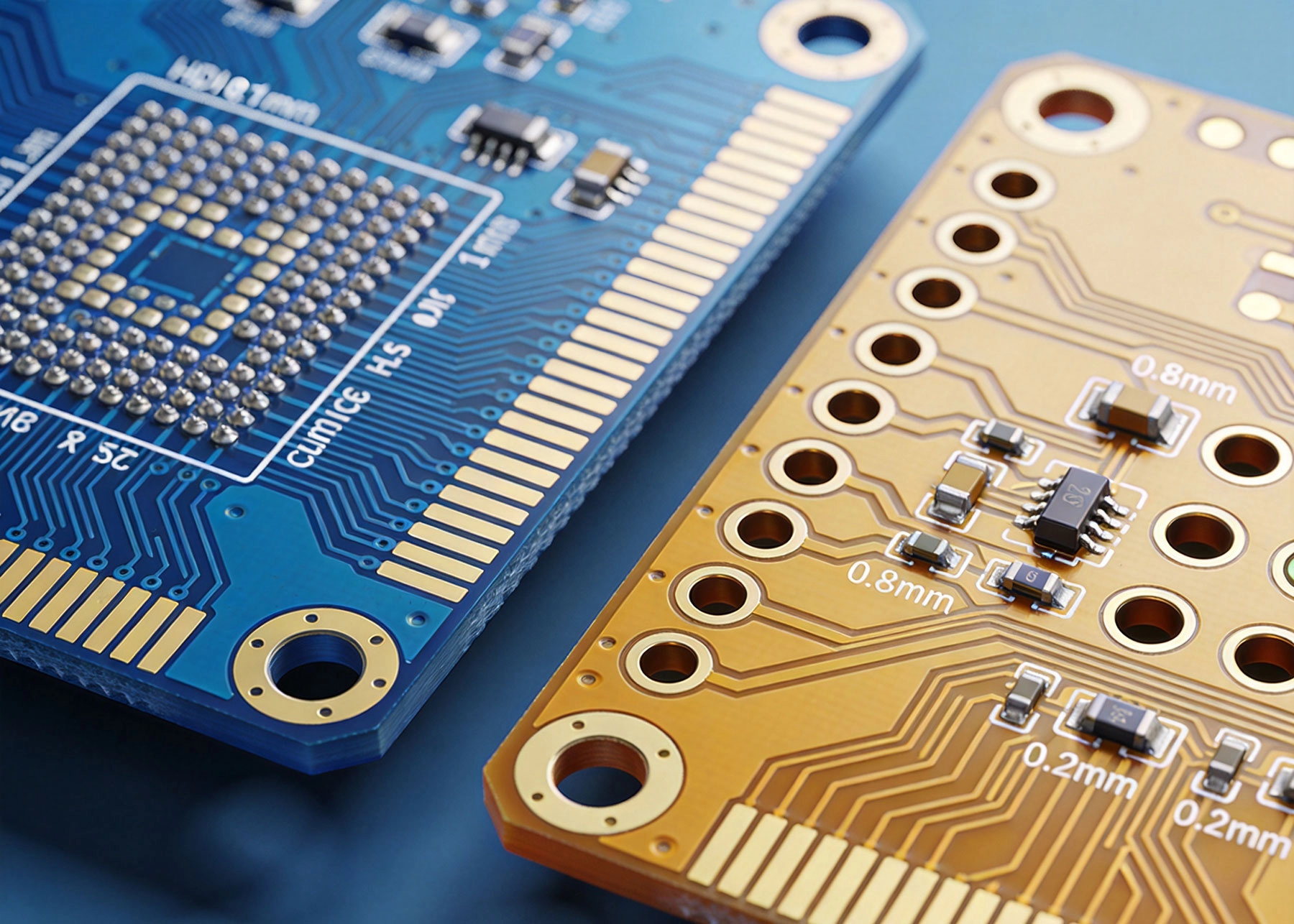
Traditional PCBs are what most people picture when they think of circuit boards—multi-layer structures with through-hole vias connecting layers, relatively coarse trace and space geometries, and manufacturing processes that have been refined over decades. These boards use mechanical drilling to create vias that connect all layers of the stack, which means every layer gets electrically connected through the entire board thickness.
The technology matured in the 1980s and 1990s, and the processes are highly optimized. Equipment is widespread, manufacturing expertise is abundant, and costs are well-understood. For many applications, traditional PCBs remain the right choice—sometimes definitively so.
Traditional PCBs rely on through-hole vias as the primary method for layer-to-layer interconnection. These vias are drilled through the entire board and then plated with copper to create electrical connections. The drilling process uses mechanical drills, and hole sizes are limited by the aspect ratio—the ratio of board thickness to drill diameter. A board that's 1.6mm thick with 0.3mm holes has an aspect ratio of about 5:1, which is manageable. Push to 0.2mm holes on the same board, and you're at 8:1, which strains many fab shops' capabilities.
Through-hole vias also consume routing space on every layer they pass through. If you have a 6-layer board, a through-hole via takes up real estate on all six layers, even if you only needed connections between layers 1 and 3. This inefficiency compounds as designs become denser.
Traditional PCB fabrication typically handles trace widths down to about 0.1mm (4 mils) reliably, with spacing to match. This is perfectly adequate for many applications—consumer electronics, industrial controls, most IoT devices. But as products shrink and functionality grows, these geometries become limiting factors rather than practical constraints.
Hdi Technology introduces several capabilities that traditional boards can't match, at least not efficiently. The core innovation is the Microvia—dramatically smaller vias that only connect adjacent layers rather than the entire board stack. This single difference cascades through the entire board architecture and design approach.
HDI is defined by IPC standards as boards with vias ≤ 0.15mm diameter and trace widths/spacing ≤ 0.1mm. But the real significance goes beyond just hitting numbers—it's about what becomes possible when you can place vias without consuming space on every layer.
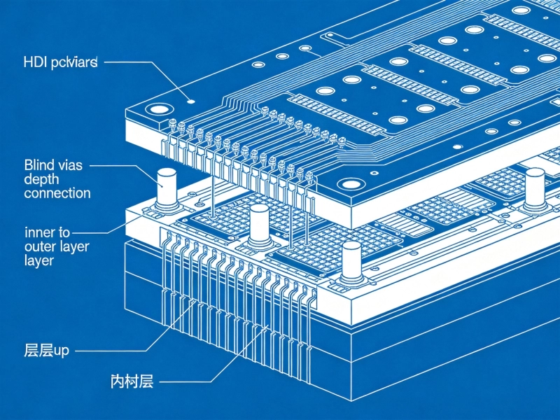
Hdi Boards typically use one or more of these Microvia types:
These aren't just smaller versions of through-hole vias—they require different manufacturing processes. Microvias are typically laser-drilled rather than mechanically drilled, which enables the smaller diameters and tighter tolerances. The plating processes are also different, optimized for filling or capping small holes rather than plating through long mechanical holes.
Most Hdi Boards require Sequential Lamination—building up the board in stages rather than drilling and plating everything at once. You might start with a core, add build-up layers with Microvias, cure, then add more layers. This adds manufacturing steps, complexity, and cost, but it enables routing densities and via placements that simply aren't possible with traditional single-shot processing.
The trade-off is clear: HDI costs more per square centimeter and requires more sophisticated manufacturing capabilities, but it delivers routing efficiency and Miniaturization that traditional boards can't match.
Consider a simple example: you need to connect layer 1 to layer 4 in a 6-layer board. In traditional technology, one through-hole via handles this, consuming space on all six layers. In HDI, you might use stacked microvias (connecting 1-2, 2-3, 3-4 in sequence) or skip vias that anchor to specific layers. The HDI approach uses less total board area, particularly in the inner layers where routing density matters most.
This efficiency matters enormously when you're working with fine-pitch components like 0.4mm BGA packages. Traditional boards often can't fan out all the connections from such packages without using multiple routing layers and complex trace routing. HDI makes this straightforward.
Here's a practical difference that surprises many designers: the same functional board can often be built with fewer layers in HDI than in traditional technology. The improved routing efficiency means you can achieve the same connectivity in 4 HDI layers as you might need in 6-8 traditional layers. Fewer layers means thinner boards, lighter weight, and potentially lower material cost despite the higher per-layer HDI processing cost.
This is why HDI frequently appears in smart phones, tablets, and wearable devices—the layer reduction directly translates to thickness and weight savings that matter in consumer electronics.
Through-hole vias in traditional boards actually help with heat spreading—the Copper Plating through the board provides Thermal Conductivity from component pads to internal planes and ultimately to heat sinks or Thermal Vias. HDI microvias, being smaller and often selectively placed, don't provide the same thermal spreading automatically.
If Thermal Management is a primary concern (high-power components, high ambient temperatures), traditional boards may offer inherent advantages that are harder to replicate in HDI without explicit thermal via design. That said, HDI designs can include thermal considerations—it's not that HDI can't handle heat, but it requires more deliberate design attention to thermal paths.
For high-speed digital signals, the shorter stubs created by microvias in HDI designs actually improve Signal Integrity compared to through-hole vias. A through-hole via from layer 1 to layer 6 in an 8-layer board creates a long stub on layers 2-5 that acts as an antenna and resonance point. HDI blind and Buried Vias eliminate these stubs, reducing parasitic capacitance and improving return loss.
This makes HDI inherently better suited for high-speed digital applications—DDR5 memory interfaces, high-speed serializers/deserializers, and RF switching networks all benefit from the improved via geometry.
Traditional PCB pricing follows a relatively predictable curve: more layers cost more, larger boards cost more, tighter tolerances cost more. The manufacturing base is large and competitive, so pricing is well-established across most specifications.
HDI pricing is more complex. The Sequential Lamination process means fewer boards fit through the factory in a given time, and the laser drilling and advanced imaging equipment represents significant capital investment. HDI boards typically cost 2-5x more per square centimeter than equivalent traditional boards. However, if you need fewer HDI layers to achieve the same function, the cost comparison can narrow significantly.
Designing for HDI requires different tools and mindsets than traditional Pcb Design. This isn't just about setting tighter design rules—it's about rethinking how you approach routing, via placement, and layer assignment.
Any modern EDA tool can design both traditional and HDI boards, but HDI designs benefit from tools with good microvia support and the ability to visualize complex via stacks. Most professional tools handle this well. The more significant issue is that HDI designs often require more design iterations due to the complexity, and the tools that best support HDI tend to be at the higher end of the market.
HDI designs require specification of via-to-pad connections, stack orientation for stacked microvias, and careful management of antipad structures on planes. These aren't difficult concepts, but they require attention that traditional board design often doesn't. You also need to think about sequential build-up constraints—if you plan to mount components on both sides of an HDI board, the layer stack sequence matters for thermal and mechanical reasons.
Despite HDI's capabilities, traditional boards remain the right choice for many applications:
If you're building industrial controls, Automotive Electronics beyond advanced driver assistance, basic IoT devices, or anything where board area isn't precious and cost is the primary driver, traditional PCBs are almost certainly the right call. The manufacturing base is larger, the expertise is more accessible, and the pricing is more predictable.
Hdi Technology delivers clear advantages in specific scenarios:
The decision typically comes down to a simple question: does the miniaturization, weight savings, or electrical performance benefit justify the higher per-board cost? If you're fitting your board into a watch or phone, the answer is clearly yes. If you're designing an industrial controller that goes into a 2kg enclosure, probably not.
HDI makes less economic sense at very high volumes than traditional boards for most applications. The higher processing cost doesn't scale down as efficiently, and traditional board manufacturing scales very well. Volume production of millions of units almost always favors traditional technology unless miniaturization requirements are absolute.
For prototyping and low-to-medium volume production, the equation shifts. If you're building 100-10,000 units of a product that fits HDI's sweet spot, the performance and size benefits often justify the cost. The key is running the numbers for your specific application rather than assuming one technology dominates.
The choice between HDI and traditional PCB technology isn't about which is better—it's about which fits your application:
Neither technology is universally superior. The electronics industry uses both extensively because both serve real needs. HDI continues to gain ground as products shrink and component packages densify, but traditional PCBs aren't going anywhere. Know your application requirements, run the cost analysis, and choose accordingly.
Yes, and this is common in practice. Many HDI boards include some through-hole vias for certain connections, particularly for larger components or where thermal paths matter. The manufacturing process accommodates both via types, though it adds complexity. This hybrid approach can optimize cost by using traditional vias where they work fine and HDI microvias where routing density requires it.
Most fab shops handle 0.1mm traces and spacing reliably. Some specialty shops push to 0.075mm or even 0.05mm for fine-line digital work. For through-hole vias, practical minimums are around 0.2mm diameter for standard boards, limited by aspect ratio considerations. If you need tighter geometries than this, you're into HDI territory.
It depends on the layer count reduction you achieve. A board that would be 1.6mm thick as an 8-layer traditional design might be 0.8mm as a 4-layer HDI equivalent. Common thickness reductions are 30-50% for designs that migrate successfully. The actual reduction depends on whether layer count reduction is achievable and practical for your routing requirements.
No inherent reliability difference exists. HDI boards undergo the same qualification testing and can achieve equivalent or better reliability depending on the design. The different thermal expansion characteristics of build-up materials can create challenges in some applications, but these are manageable with proper design. Military and aerospace applications use HDI successfully when the application warrants it.
HDI boards typically require 2-4 weeks longer than equivalent traditional boards due to the sequential lamination process. Traditional boards are often available in 1-2 weeks from many suppliers. If you're working with tight development schedules, this lead time difference matters. Plan accordingly, particularly for prototypes where quick turns may not be available for HDI.
Designing Automotive HDI Boards for Vibration and Shock ResistanceJuly/17/2026

The Role of HDI in Avionics and Flight Control SystemsAugust/13/2026

How HDI Technology Supports Advanced Driver Assistance Systems (ADAS)June/25/2026
The Role of HDI in Robotics and Motion Control SystemsAugust/10/2026
HDI Solutions for In-Vehicle Infotainment (IVI) and ClustersAugust/07/2026
Critical Quality Checkpoints in the HDI Production LineJuly/13/2026
Understanding HDI Terminology: A Glossary for EngineersAugust/03/2026
Exploring the 6 Types of HDI Structures: From Type I to Any-LayerAugust/14/2026