
The smartphone in your pocket is a marvel of Miniaturization. Within its slim profile, dozens of chips, thousands of components, and miles of copper traces work together to deliver computing power that would have seemed like science fiction just two decades ago. At the heart of this technological achievement lies a Pcb Technology that's been quietly revolutionizing electronics: HDI PCBs.
High Density Interconnect (HDI) PCBs aren't just incremental improvements over traditional circuit boards. They represent a fundamental shift in how engineers design and manufacturers build the electronic foundations of modern devices. For smartphone manufacturers, Hdi Technology isn't optional—it's the enabling technology that makes next-generation devices possible.
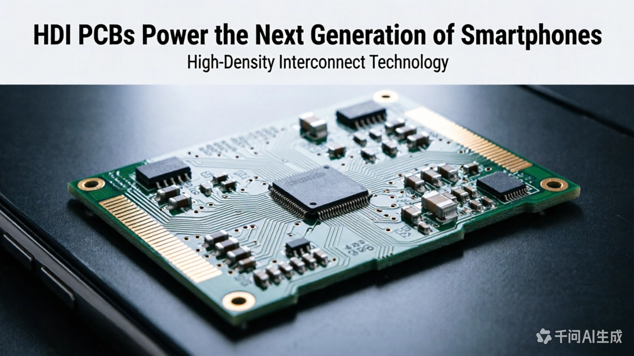
Traditional rigid PCBs use through-hole vias that connect every layer from top to bottom. While functional, this approach has significant limitations for smartphones:
HDI PCBs address these limitations through advanced manufacturing techniques that enable:
A modern flagship smartphone might use a 10-layer Any-layer Hdi board with the following characteristics:
Micro Vias connect adjacent layers throughout the stack, while select through vias provide critical ground references. This architecture enables designers to optimize each layer for specific functions while maintaining Signal Integrity across the entire system.
Smartphone Pcb designers must balance multiple competing requirements:
Modern Hdi Boards often use Sequential Lamination—building the board in multiple stages rather than all at once. This allows:
Laser Drilling creates vias that mechanical drilling simply cannot achieve:
The trade-off? Laser Drilling is significantly more expensive than mechanical drilling and requires specialized equipment and expertise. This cost drives the premium pricing of Hdi Boards compared to conventional alternatives.
The Any-layer Hdi (sometimes called "any-layer interconnects" or ALIVH) approach represents the pinnacle of Smartphone Pcb technology. Any-layer boards allow micro vias to connect any two adjacent layers, providing:
Apple popularized any-layer Hdi Technology with the iPhone 4, and it has since become standard in flagship smartphones from Samsung, Huawei, Xiaomi, and other major manufacturers.
5G smartphones require sophisticated antenna systems operating at frequencies up to 100 GHz in some markets. HDI PCBs provide:
The high frequency performance of HDI substrates—often featuring low dielectric constants and dissipation factors—minimizes signal loss at mmWave frequencies.
Neural processing units (NPUs) and AI accelerators demand:
HDI technology meets these requirements through optimized layer assignment, ground plane placement, and power plane design that would be impossible with conventional board construction.
Modern flagship smartphones feature 3-5 camera modules with sophisticated image processing. HDI PCBs support:
Wireless charging introduces unique PCB challenges:
Hdi Manufacturing requires extraordinary process control. A single particle contamination event can destroy a multi-layer board worth $50-200. Leading manufacturers address this through:
Smartphone Pcb Materials must balance multiple properties:
Most smartphone HDI boards use modified epoxy or resin systems optimized for laser Micro Via formation. These materials require careful handling and processing to achieve consistent results.
Every HDI board undergoes rigorous testing before assembly:
Smartphone Pcb Technology has evolved rapidly:
Emerging trends shaping smartphone Pcb Evolution include:
Not all HDI manufacturers can support flagship smartphone production:
When qualifying an HDI supplier for smartphone applications, ask:
Most flagship smartphones use 8-12 layer HDI PCBs, with trend toward higher counts as functionality increases. The iPhone series, for example, has evolved from 6-8 layers in earlier models to 10-12 layers in recent generations. Mid-range smartphones typically use 6-8 layers, while budget devices may use conventional 4-6 layer boards.
HDI boards command premium pricing due to specialized manufacturing requirements: laser drilling equipment costing millions of dollars, clean room environments, sequential lamination processes, and extremely tight process tolerances. Additionally, material costs for low-loss HDI substrates exceed standard FR-4. The investment is justified by the ability to pack more functionality into smaller spaces—a critical advantage in competitive smartphone markets.
Standard HDI uses micro vias to connect adjacent layers only. Any-layer HDI (or any-layer IVH - Interstitial Via Hole) allows micro vias to connect any two layers in the stack, providing maximum design flexibility. Any-layer technology typically requires more complex sequential lamination but enables reduced layer counts and improved signal routing compared to standard HDI approaches.
When properly designed and manufactured, HDI PCBs offer excellent reliability. The reduced stub lengths of micro vias actually improve high-frequency signal integrity compared to through-hole designs. Buried vias eliminate exposed barrel surfaces that can crack under thermal stress. Modern HDI boards routinely pass drop tests, thermal cycling, and mechanical vibration requirements specified by smartphone OEMs. The key is selecting a manufacturer with proven smartphone production experience.
Absolutely. HDI technology continues to evolve in several directions: ultra-thin dielectrics enabling thinner boards, embedded passives reducing component count, advanced Low-loss Materials for 6G frequencies, and improved thermal management for AI processors. While alternative technologies like substrate-like PCBs (SLP) compete for some applications, HDI remains the foundation for mainstream smartphone PCB technology and will continue advancing alongside device requirements.
HDI PCBs are the unsung heroes of modern smartphone technology, enabling the functionality, performance, and miniaturization that consumers expect. Understanding HDI technology isn't just for PCB engineers—it's essential knowledge for anyone working to develop or specify next-generation mobile electronics.
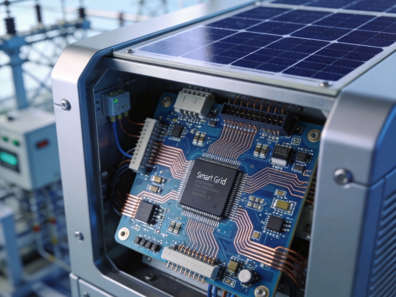
The Role of HDI in Smart Grid and Energy Storage SystemsAugust/06/2026
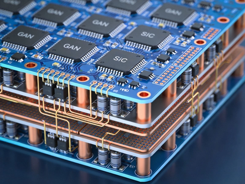
Challenges of Integrating HDI in High-Efficiency Power InvertersJuly/16/2026
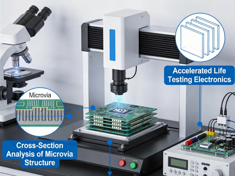
Key Factors Influencing the Long-Term Reliability of HDI PCBsMay/28/2026
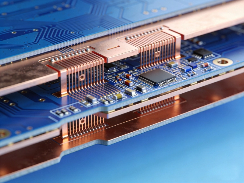
How HDI Technology Enables the Miniaturization of Modern ElectronicsSeptember/20/2026
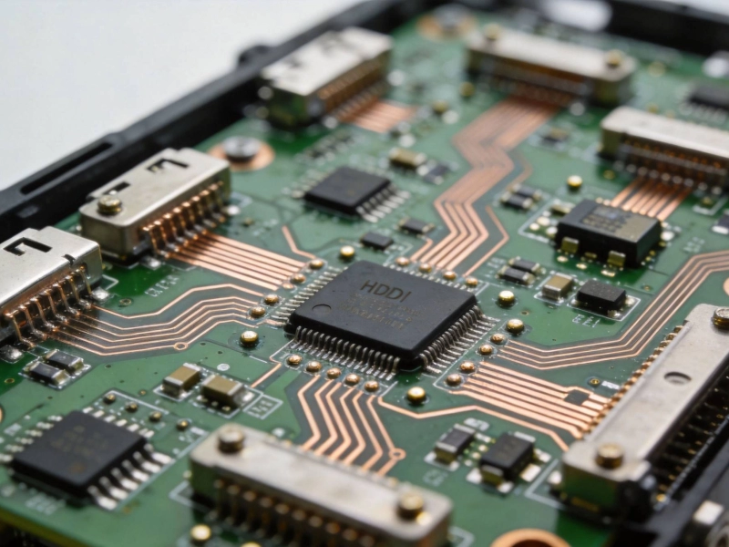
HDI Applications in Advanced Battery Management Systems (BMS)June/18/2026
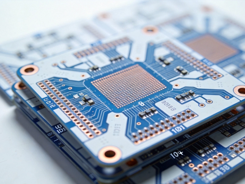
How Manufacturers Achieve High Precision Alignment in 10+ Layer HDI BoardsAugust/15/2026
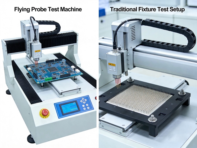
Flying Probe vs. Fixture Testing: Which is Best for HDI PCBs?June/11/2026
Managing Layer-to-Layer Registration Accuracy in Multilayer HDIOctober/09/2026