Open Nav

The battery management system sits at the heart of every electric vehicle and grid energy storage installation. As these markets accelerate globally, the electronics driving battery safety, efficiency, and longevity face unprecedented demands. Hdi Pcb technology has emerged as the enabling foundation for next-generation BMS designs, packing more functionality into smaller spaces while meeting the reliability requirements that safety-critical automotive applications demand. Understanding how Hdi Applications serve BMS development prepares engineers and procurement teams to make better architectural decisions.
Chinese manufacturers have invested heavily in HDI capability to serve the exploding EV market. Facilities in Shenzhen, Guangzhou, and other manufacturing hubs now produce sophisticated Hdi Boards that rival quality from any global supplier. This manufacturing capacity creates opportunities for Western companies to access advanced BMS electronics at competitive prices. But realizing these opportunities requires understanding the technical requirements that HDI in BMS applications demands.
This comprehensive exploration covers why Hdi Technology matters for BMS, how specific HDI structures serve BMS functions, and what engineering considerations guide successful BMS HDI implementations. Whether you're designing a new BMS architecture or sourcing existing designs, this information helps you navigate decisions that affect battery safety and performance.
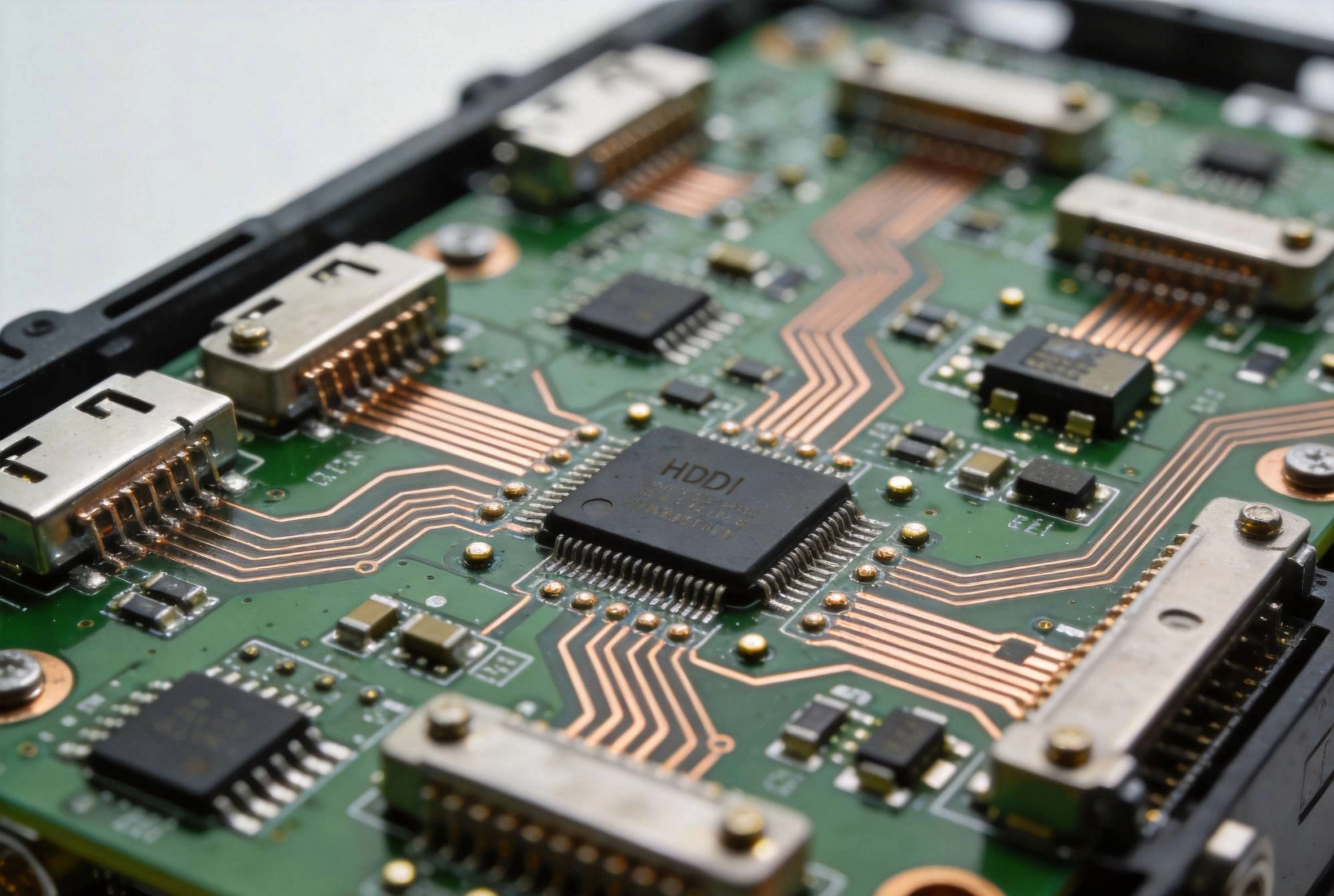
A battery management system monitors and controls rechargeable battery packs. Its core responsibilities include cell voltage monitoring, temperature measurement, state-of-charge estimation, cell balancing, and protection against abuse conditions. In electric vehicles, BMS circuits must process data from hundreds of individual cells while maintaining communication with vehicle control systems and charging infrastructure.
The electronics required for these functions include analog front ends for cell measurement, digital processors for algorithms, communication transceivers for vehicle networks, gate drivers for balancing circuits, and power conversion stages for system power. Each functional block presents Pcb Design challenges that Hdi Technology helps address. The density requirements for automotive BMS push beyond what conventional Pcb Technology can deliver economically and reliably.
Beyond density, BMS PCBs must operate in challenging environments. Battery packs experience temperature ranges from -40°C to 85°C or wider. Vibration and mechanical shock stress connections. Electromagnetic interference from Power Electronics can corrupt sensitive measurement signals. HDI construction provides inherent advantages for addressing these environmental challenges, making it the natural choice for advanced BMS implementations.
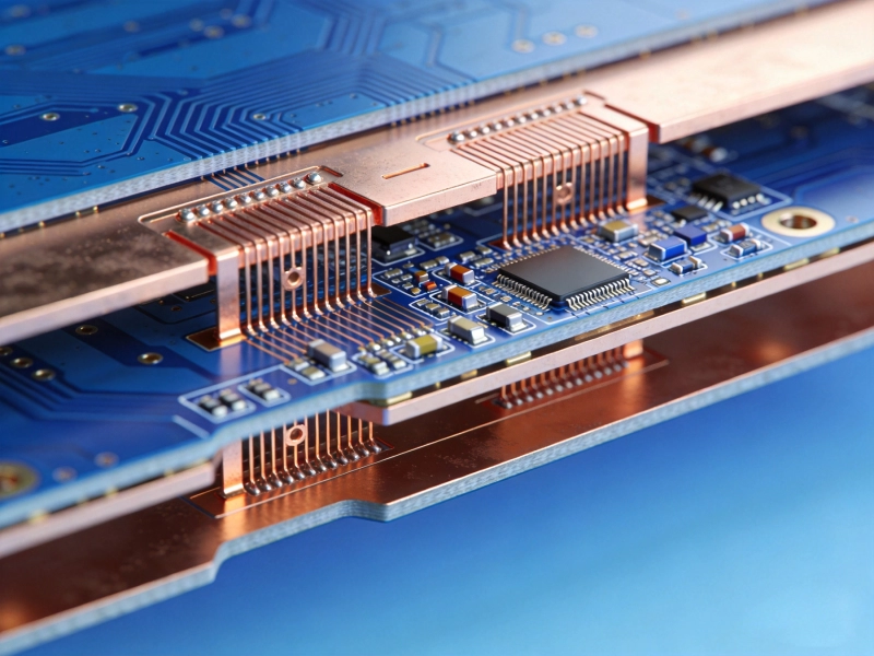
High Density Interconnect PCBs employ Microvias, finer trace geometries, and higher wiring density than conventional multilayer boards. These capabilities matter enormously for BMS applications where board real estate costs money and weight. A typical automotive BMS might need to monitor 100 cells or more in a vehicle battery pack. Accommodating all the measurement channels, processors, and communication interfaces in a compact form factor demands HDI construction.
The Microvia Technology central to HDI enables blind and Buried Via structures that dramatically reduce board area. A conventional through-hole via occupies space on every layer it passes through. A Blind Via connects only the surface to an inner layer, while a Buried Via connects inner layers without touching the surfaces. These structures allow components to be placed more densely and traces to route more efficiently. For BMS boards that must fit within battery pack envelopes, HDI's area efficiency becomes essential rather than merely advantageous.
Signal Integrity in BMS applications benefits significantly from HDI construction. Shorter interconnection lengths reduce inductance and improve noise immunity for the sensitive analog measurement signals that determine state-of-charge accuracy. The finer trace geometries available in HDI allow controlled impedance lines to be routed more precisely, improving high-speed communication signal quality. These electrical advantages translate directly into BMS measurement precision and communication reliability.
Successful HDI BMS designs start with thoughtful stack-up planning. The layer structure determines routing options, via capabilities, and manufacturing cost. Automotive BMS typically employ 4 to 8 layer HDI constructions, though more complex systems may use additional layers. The specific configuration depends on component count, routing complexity, and thermal requirements.
A common BMS HDI stack-up employs Sequential Lamination with multiple buildup layers. The core structure provides mechanical stability and ground plane planes, while buildup layers accommodate high-density component areas. For example, a six-layer HDI BMS board might have a four-layer core with two buildup layers on each side. This construction provides excellent routing flexibility while maintaining manufacturability at Chinese facilities.
Thermal Management requires consideration during Stack-up Design. BMS electronics generate heat from processors, MOSFETs in balancing circuits, and communication transceivers. The stack-up should include dedicated power and ground planes that serve as heat spreading layers. Thermal Vias can connect Thermal Pad components to these planes, moving heat away from sensitive devices. Stack-up decisions made early in design profoundly affect Thermal Performance at the system level.
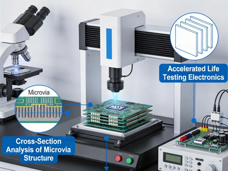
Microvia Reliability in automotive applications requires careful attention to design rules and manufacturing quality. The primary failure mechanism in Microvias involves thermal cycling— the via structure experiences stress as the board temperature changes. HDI manufacturers serving automotive customers have developed processes that pass rigorous automotive reliability testing including thermal shock, thermal cycling, and vibration exposure.
Via-in-pad construction frequently appears in BMS designs. This technique places vias directly in component pads, eliminating the inductance and resistance of traditional via-to-pad connections. For high-current measurement lines and power connections in BMS, Via-in-pad improves electrical performance. However, via-in-pad requires specialized manufacturing processes including Via Filling and plating that not all Chinese HDI facilities offer reliably. Verify your manufacturer's capability and Quality Control for via-in-pad structures before specifying them.
Aspect ratio limits constrain Microvia geometry. The ratio of depth to diameter determines whether a Microvia can be manufactured reliably. Standard microvia guidelines specify aspect ratios of 0.8:1 or 1:1, though advanced processes can achieve slightly higher ratios. For BMS boards with thicker cores, these limits may require additional buildup layers rather than deeper microvias. Your HDI manufacturer can recommend optimal microvia specifications based on your stack-up.
The components placed on BMS Hdi Boards span a wide range of package types. High-pin-count ICs like BMS analog front ends and microcontrollers typically employ BGA or QFN packages. These packages benefit enormously from HDI's fine line and microvia capabilities, enabling fan-out from tight pitch pins to routing layers without breaking into conventional trace widths.
Passive components increasingly migrate to 0201 and 01005 packages on advanced BMS designs. These tiny components save board area but present manufacturing challenges. Chinese assembly houses with modern equipment routinely handle these small components, but placement accuracy requirements are stringent. HDI's flat surface characteristics facilitate reliable placement of these miniature components, though paste volume control becomes more critical.
Automotive-grade components carry specific qualification requirements. The Aec-q100 standard for integrated circuits and AEC-Q200 for passives define test sequences that verify reliability under automotive stress conditions. When specifying components for BMS applications, confirm that your manufacturer understands and stocks automotive-grade parts. Using commercial-grade components in automotive BMS applications creates liability and reliability risks that outweigh any cost savings.
Electromagnetic interference poses significant challenges in BMS environments. High-current power switching in battery charging and discharging generates conducted and radiated emissions. Simultaneously, the BMS must measure microvolt-level signals from battery cells without corruption. HDI construction provides inherent EMI advantages that help address these conflicting requirements.
Ground plane integrity in HDI stack-ups supports effective shielding. The multiple plane layers available in HDI constructions allow dedicated shielding layers for sensitive analog sections. Separating digital noise sources from analog measurement circuits on different layers with ground between them reduces cross-talk and interference. Your Stack-up Design should partition these functions deliberately rather than mixing them arbitrarily.
Feedback loops and control lines in BMS switching circuits require careful routing. The high-frequency components of switching waveforms can couple into sensitive measurement circuits if routing isn't controlled. HDI's controlled impedance capabilities and precise trace geometry control enable predictable crosstalk behavior that can be designed around. Without HDI's precise dimensions, these coupling paths become more variable and harder to manage.
China's Hdi Manufacturing capability has matured dramatically over the past decade. Major Chinese PCB manufacturers now operate facilities that produce automotive-qualified HDI boards meeting the most demanding international standards. The Iatf 16949 automotive Quality Management System certification is increasingly common among Chinese suppliers serving the EV market.
When evaluating Chinese HDI manufacturers for BMS applications, verify specific capabilities beyond general HDI designation. Ask about their experience with automotive BMS production— volume, complexity, and quality outcomes. Request references from other BMS customers if possible. The learning curve for Automotive Hdi is steep; manufacturers with proven track records offer lower risk than those attempting their first BMS projects.
Documentation requirements deserve explicit attention. Chinese manufacturers may need guidance on automotive documentation standards including PPAP (Production Part Approval Process), FMEA documentation, and process control specifications. Establishing these requirements clearly in your supplier agreement prevents quality surprises during production. Many Chinese manufacturers have experience with Western automotive requirements and can guide you through the documentation expectations.
HDI construction costs more than conventional multilayer PCBs, but the system-level economics often favor HDI despite higher board costs. A board that uses HDI to integrate functions that would otherwise require multiple boards saves assembly cost, connectors, cables, and enclosure space. When evaluating HDI for BMS, consider total system cost rather than board cost alone.
Volume dramatically affects HDI pricing. Chinese manufacturers offer significant economies of scale for high-volume BMS production. Prototype and low-volume HDI boards carry substantially higher per-unit costs due to setup amortization. If your BMS production volumes justify HDI integration, work with your manufacturer to optimize the transition from prototype to production pricing. Some Chinese suppliers offer prototype pricing programs that reduce initial costs while you qualify the design.
Test and inspection costs factor into total HDI economics. The dense component placement and complex routing in HDI boards may require additional test coverage including AOI (Automated Optical Inspection) and X-ray Inspection for hidden solder joints. These inspection steps add cost but catch defects before they reach customers. The right inspection strategy balances cost against defect escape risk based on your application reliability requirements.
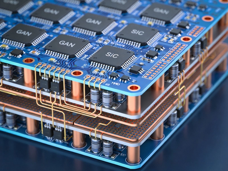
As battery technologies advance, BMS electronics evolve to match. Solid-state batteries promise higher energy density but introduce new measurement challenges. Silicon carbide and gallium nitride power devices enable faster charging but generate different EMI environments. HDI technology continues advancing to address these emerging requirements.
Embedded component technology represents an emerging HDI frontier for BMS applications. Components embedded within the PCB structure rather than mounted on surfaces could further reduce BMS board size and improve reliability. Some Chinese manufacturers are developing embedded component capabilities specifically for automotive applications. While still emerging, this technology may become important for next-generation BMS architectures.
Automotive functional safety requirements under ISO 26262 influence BMS architecture decisions. These standards demand specific levels of hardware fault tolerance and diagnostic coverage. HDI construction can support redundant measurement channels and diagnostic features that enable ASIL (Automotive Safety Integrity Level) compliance. As safety requirements become more stringent, HDI's flexibility in implementing redundant structures becomes increasingly valuable.
HDI technology has become essential for advanced battery management systems. The density, Signal Integrity, and reliability advantages that HDI provides match perfectly with BMS requirements for compact form factors, precise measurements, and automotive-grade durability. Chinese manufacturers have invested heavily in HDI capability to serve the exploding EV market, creating opportunities for companies worldwide to access world-class HDI BMS electronics.
Successful HDI BMS development requires attention to fundamentals: thoughtful stack-up design, appropriate microvia specifications, component selection that matches manufacturing capabilities, and EMI mitigation strategies that address the challenging BMS environment. Working with Chinese manufacturers requires clear communication of Automotive Quality requirements and documentation expectations. The investment in proper specification pays dividends through reliable products and stable manufacturing relationships.
As electric vehicle adoption continues accelerating globally, the BMS electronics market grows correspondingly. HDI technology provides the foundation for BMS innovation, enabling more cells monitored, tighter battery utilization, and safer operation. Engineers and procurement professionals who understand Hdi Applications in BMS position their organizations to capitalize on the electric future.
How HDI Technology Enables the Miniaturization of Modern ElectronicsSeptember/20/2026

How HDI PCBs Power the Next Generation of SmartphonesJune/17/2026
Key Factors Influencing the Long-Term Reliability of HDI PCBsMay/28/2026
Challenges of Integrating HDI in High-Efficiency Power InvertersJuly/16/2026
The Role of HDI in Smart Grid and Energy Storage SystemsAugust/06/2026

How HDI Technology Supports Advanced Driver Assistance Systems (ADAS)June/25/2026
Conductive Anodic Filament (CAF) Resistance in High-Density BoardsJuly/31/2026
How to Measure and Control Impedance Tolerance in HDI BoardsAugust/03/2026