
Every electronic product carries an implicit promise: it will work reliably for its intended service life. For a smartphone, that might mean 3-5 years of daily use. For an automotive electronic control unit, it's 15+ years and 150,000 miles of operation. For industrial equipment in factory automation, lifetimes of 20 years are expected. Meeting these requirements is far from automatic — it demands understanding and controlling the key factors that influence Hdi Pcb reliability. Unlike standard multilayer PCBs, High-density Interconnect boards face unique reliability challenges arising from their fine features, layered construction, and the thermal and mechanical stresses that accumulate over years of operation. This guide examines every major factor affecting Hdi Pcb long-term reliability, from material properties to design practices to manufacturing process controls, so you can build products that last.
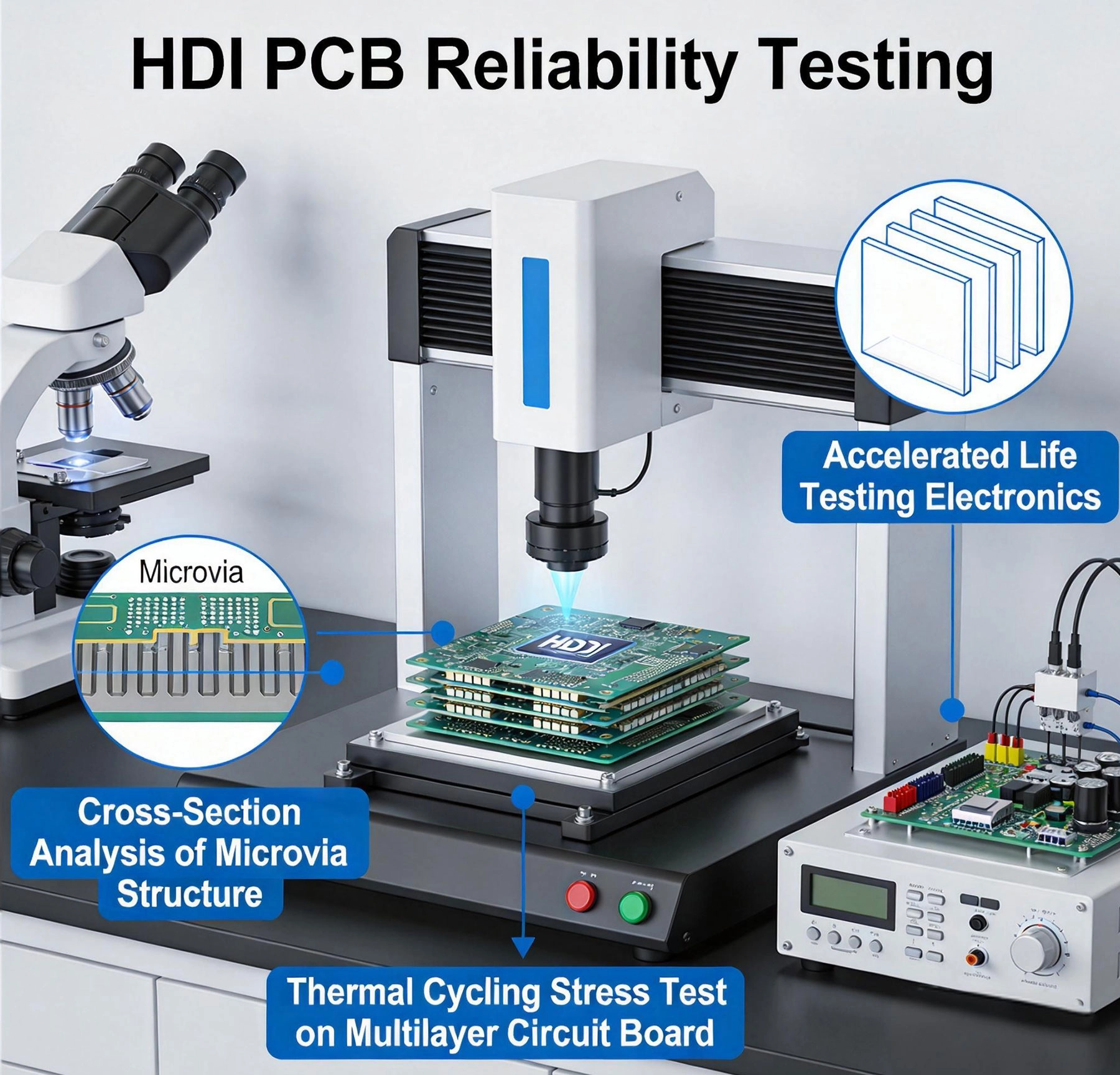
Before examining specific factors, it's important to understand what "reliability" means in the context of HDI PCB performance. Reliability is the probability that a product will function correctly over a specified time under specified operating conditions. For HDI PCBs, this translates to maintaining electrical continuity, insulation resistance, and mechanical integrity throughout the product's service life.
HDI PCBs face reliability challenges that conventional boards do not. The Microvia — the defining feature of Hdi Technology — is simultaneously the technology's greatest strength and its greatest reliability vulnerability. A Microvia with a 0.15mm diameter and 0.1mm thickness must survive thousands of thermal cycles between -40°C and +125°C without cracking. The thin dielectrics between HDI layers (often 50-100 microns) must maintain isolation under voltage stress while absorbing differential expansion stresses from the materials around them. These are engineering challenges that require careful attention to every factor that influences HDI durability.
10-20 Years
-40°C to +125°C
500-2000
Microvia Crack
The microvia is the heart of Hdi Technology and the element most prone to reliability failure. Unlike through-hole vias in conventional PCBs, Microvias are blind or buried connections between adjacent layers, with aspect ratios (depth to diameter) that create unique mechanical stress concentrations. Understanding and controlling microvia integrity is foundational to Hdi Reliability.
Coefficient of thermal expansion (CTE) mismatch is the primary driver of Hdi Reliability failures. Every material in an HDI assembly has a different CTE — the rate at which it expands when heated and contracts when cooled. When these different materials are bonded together and subjected to temperature changes, differential expansion creates stress at every interface. Over thousands of thermal cycles, these cyclic stresses cause fatigue failures.
| Material | CTE (ppm/°C) in X-Y plane | CTE (ppm/°C) in Z-axis | Reliability Implication |
|---|---|---|---|
| Copper | 17 | 17 | Reference — high expansion |
| Standard FR-4 | 14-18 | 50-100 | High Z-axis expansion creates via stress |
| High-Tg FR-4 | 12-16 | 30-60 | Improved over standard FR-4 |
| Polyimide | 12-16 | 40-60 | Good Thermal Performance |
| Hydrocarbon Ceramic | 6-12 | 20-40 | Good CTE match to copper |
| Solder (SAC305) | 22-24 | 22-24 | High expansion — major stress source |
| Solder Mask | 30-60 | 30-60 | Variable — depends on formulation |
The PCB substrate materials you choose determine the foundation upon which all HDI reliability rests. Material properties — glass transition temperature (Tg), decomposition temperature (Td), moisture absorption, dielectric constant stability, and mechanical strength — interact to determine how well your board survives environmental stress over time.
Tg is the temperature at which the substrate transitions from a rigid, glassy state to a soft, rubbery state. Below Tg, the material is dimensionally stable but brittle. Above Tg, it becomes flexible but also expands dramatically — the CTE can increase by 3-5x above Tg. For high-reliability applications, choose materials with Tg significantly above your maximum operating temperature:
Td is the temperature at which the material begins to chemically decompose. This is typically 20-40°C above Tg. For lead-free soldering processes that reach peak temperatures of 260°C, materials with Td below 260°C risk degradation during assembly. Always specify Td > 260°C for lead-free assemblies.
FR-4 and similar materials absorb moisture from the environment (typically 0.1-0.3% by weight under normal conditions). When heated rapidly — as in solder reflow — this moisture expands to vapor, creating pressure that can cause delamination, microvia damage, or "popcorn" cracking of component packages. For high-reliability HDI assemblies:
| Property | Standard FR-4 | High-Tg FR-4 | Polyimide | Hydrocarbon Ceramic |
|---|---|---|---|---|
| Tg (°C) | 130 | 150-180 | 250-260 | 200-280 |
| Td (°C) | 320 | 340-360 | 380-400 | 380-420 |
| CTE X-Y (ppm/°C) | 14-18 | 12-16 | 12-16 | 6-12 |
| Dielectric Constant (1MHz) | 4.2-4.5 | 4.0-4.5 | 3.5-4.2 | 3.0-4.0 |
| Cost Index | 1.0 | 1.2-1.5 | 3-5 | 2-4 |
| Best For | Consumer | Industrial/Auto | Harsh Env. | High-Speed/Hi-Rel |
Thermal cycling is the primary environmental stressor for HDI PCBs. Every power-on, power-off, and ambient temperature change subjects the assembly to a cycle of expansion and contraction. The damage is cumulative — each cycle causes a small amount of fatigue damage, and after enough cycles, the accumulated damage exceeds the material's fatigue limit, causing failure.
| Environment | Temp Range | Typical Cycles/Year | HDI Requirements |
|---|---|---|---|
| Consumer Indoor | 0°C to 40°C | 500-1,000 | Standard materials, basic design |
| Consumer Handheld | -10°C to 50°C | 1,000-2,000 | High-Tg materials, good design |
| Industrial Indoor | -25°C to 70°C | 1,000-3,000 | High-Tg or better, robust design |
| Automotive Engine Bay | -40°C to 125°C | 3,000-5,000 | Polyimide or better, Aec-q100 |
| Aerospace | -55°C to 85°C (cabin) | 5,000-10,000 | High-reliability materials, full qualification |
| Downhole Oil/Gas | -40°C to 175°C | Varies | Specialized materials, custom qualification |
The most carefully designed HDI board will fail prematurely if manufacturing processes introduce defects or inconsistencies. Manufacturing process control is a critical factor in HDI PCB long-term reliability — arguably as important as material selection or design choices. The processes that most significantly affect HDI reliability are those that create the microvia structure and the solder interconnections.
HDI microvias are typically formed by laser ablation — using a UV or CO2 laser to remove Dielectric Material and create the via barrel. The quality of this process directly determines via reliability:
Copper Plating in microvias must meet stringent quality requirements for HDI reliability. Key parameters include:
Sequential Lamination of Hdi Boards creates multiple high-temperature exposures that can affect material properties and introduce defects:
Design for reliability (DFR) applies reliability engineering principles to the Pcb Design process, making deliberate choices that improve the board's ability to survive environmental stress throughout its service life. Good HDI design for reliability starts at the earliest stages of the project and informs every subsequent decision.
PCB assembly — component mounting and solder interconnection — introduces stresses that can affect long-term reliability even if the bare board is perfect. The assembly process creates the electrical and mechanical connections that must survive the product's service life, and each process step has parameters that influence reliability.
Assembly defects found before shipping don't cause field failures. Implement comprehensive inspection and test to catch defects:
Hdi Pcb Reliability qualification verifies that the design, materials, and manufacturing processes produce boards that meet the application's lifetime requirements. Qualification testing is mandatory for automotive (Aec-q100/Q200), medical (FDA), and aerospace applications, and strongly recommended for all high-reliability products.
The primary reliability test for HDI assemblies. Samples are cycled between temperature extremes while monitored for electrical opens or parameter drift. Automotive qualification typically requires 1000 cycles from -40°C to +125°C. Board-level reliability guidance is available in IPC standards (Ipc-9701 for surface mount attachments).
Samples held at 85°C / 85% relative humidity with electrical bias applied. This accelerates corrosion, dendrite growth, and moisture-related delamination mechanisms. Typical test duration: 1000 hours (equivalent to years of field exposure in harsh environments).
An accelerated version of THB using higher temperature and humidity (130°C / 85% RH or 110°C / 85% RH). Achieves similar acceleration in 96-100 hours but is more stressful and may fail mechanisms that wouldn't occur at lower stress levels. Use with caution.
For portable electronics, drop shock testing simulates the mechanical shocks of real-world use. IPC-9702 defines drop test methods for board-level reliability. High-reliability HDI designs for handheld devices should be qualified to relevant drop test standards.
Our engineering team has decades of experience designing and manufacturing high-reliability HDI PCBs for automotive, medical, industrial, and aerospace applications. We provide design for reliability analysis, material selection support, qualification testing services, and full Hdi Manufacturing with comprehensive quality assurance. Contact us to discuss your reliability requirements.
Field failure rates for well-designed HDI PCBs in consumer applications are typically in the range of 50-500 parts per million (PPM) over a 3-5 year service life. However, this varies dramatically based on the application environment, design quality, and manufacturing process control. A Smartphone Pcb with poor Thermal Management might see 2-5% failure rates over 3 years, while a well-designed automotive ECU typically achieves <100 PPM over 15 years. The key insight is that consumer products have shorter required lifetimes and lower reliability requirements than industrial or automotive products, so they can tolerate higher failure rates — but they must still be designed to meet those requirements.
Lead-free solder (primarily SAC305: 96.5% Sn, 3% Ag, 0.5% Cu) presents both advantages and challenges for Hdi Pcb Reliability. On the positive side, lead-free solder has higher melting point (217°C vs 183°C for tin-lead) which provides higher temperature margin. However, SAC305 has higher stiffness than tin-lead solder, which creates higher stress on joints under thermal cycling. Lead-free also forms thicker, more brittle intermetallic compound (IMC) layers with copper, which can be a fracture path under stress. Overall, well-designed lead-free assemblies can meet or exceed tin-lead reliability, but the design rules are different — larger pad sizes, tighter process control, and often underfill for BGAs are needed to achieve equivalent reliability.
Standard through-hole vias (plated through holes, PTH) have aspect ratios of 3:1 to 5:1 and diameters of 0.3mm or larger. Microvias in HDI have aspect ratios of 0.5:1 to 1:1 and diameters of 0.1mm to 0.3mm. The smaller geometry of microvias creates higher stress concentrations at the via-to-pad interface. However, microvias also have shorter barrel lengths (connecting adjacent layers rather than the full board thickness), which reduces the total thermal expansion strain they must accommodate. In practice, well-made microvias in HDI PCBs are typically as reliable as or more reliable than through-hole vias, because HDI construction uses thinner dielectrics with less differential expansion and because the Hdi Manufacturing process generally applies tighter process control.
PCB thickness affects reliability primarily through its influence on CTE mismatch stress. Thinner boards have less thermal mass and experience faster temperature changes, but also flex more easily, potentially distributing stress differently. For HDI assemblies, thinner boards (0.5mm-1.0mm) are more flexible and can accommodate some thermal mismatch strain through board bending. Thicker boards (1.6mm-2.0mm+) are stiffer and transfer more thermal strain directly to the solder joints and vias. The relationship is not simple — always verify thermal cycling performance with representative board thickness. For multilayer Hdi Boards, maintaining consistent thickness across the board (thickness uniformity) is as important as the absolute thickness value.
Microvia failures are among the most difficult Pcb Defects to repair, and some cannot be repaired at all. For buried microvias in the internal layers of an HDI board, there is typically no physical access for rework. For blind microvias on the surface layer, microvia rework is possible but requires specialized equipment (microvia laser ablation, precision plating) and skill. The repair success rate for surface-layer microvia defects is typically 70-90%, and repaired vias may have lower reliability than original vias. The practical answer is: design for reliability from the start rather than relying on rework to fix problems. If microvia defects are discovered during manufacturing, the board should be reworked or scrapped rather than shipped with known reliability risks.
Supplier qualification is absolutely critical for HDI reliability. The fine features and tight tolerances of HDI manufacturing require process capabilities and quality systems that not all manufacturers possess. A supplier qualification program should include: audit of process capability indices (Cpk) for critical processes; review of statistical process control data and process failure mode effects analysis (PFMEA); qualification builds to verify first-pass yield and reliability; ongoing quality monitoring and reporting. For automotive and medical applications, supplier qualification is typically required as part of regulatory compliance (Iatf 16949 for automotive, Iso 13485 for medical). Even for consumer applications, working with a qualified supplier whose processes you understand and trust is the foundation of reliable HDI products.
HDI Applications in Advanced Battery Management Systems (BMS)June/18/2026
The Role of HDI in Smart Grid and Energy Storage SystemsAugust/06/2026
Challenges of Integrating HDI in High-Efficiency Power InvertersJuly/16/2026

How HDI PCBs Power the Next Generation of SmartphonesJune/17/2026
How HDI Technology Enables the Miniaturization of Modern ElectronicsSeptember/20/2026
Top 10 Frequently Asked Questions About HDI PCB TechnologyMay/28/2026
How to Read and Interpret HDI PCB Stack-up Drawings?July/14/2026
HDI PCB Cost Guide: What Factors Drive the Price Up?June/16/2026