Open Nav

A primary focus is the structural integrity of Microvias and plated through-holes (PTH). Manufacturers must strictly control plating thickness and ensure complete Via Filling to prevent defects like voids or wall fractures during thermal expansion. Advanced Non-destructive Testing, such as 3D X-ray Inspection and Scanning Acoustic Microscopy (SAM), is employed to detect hidden internal flaws. Furthermore, boards undergo extreme environmental stress tests, including repeated thermal shock cycling and high-humidity exposure. By addressing these failure mechanisms through precise工艺 control and comprehensive testing, a High Density Interconnect PCB achieves the robust durability required for modern high-performance applications.
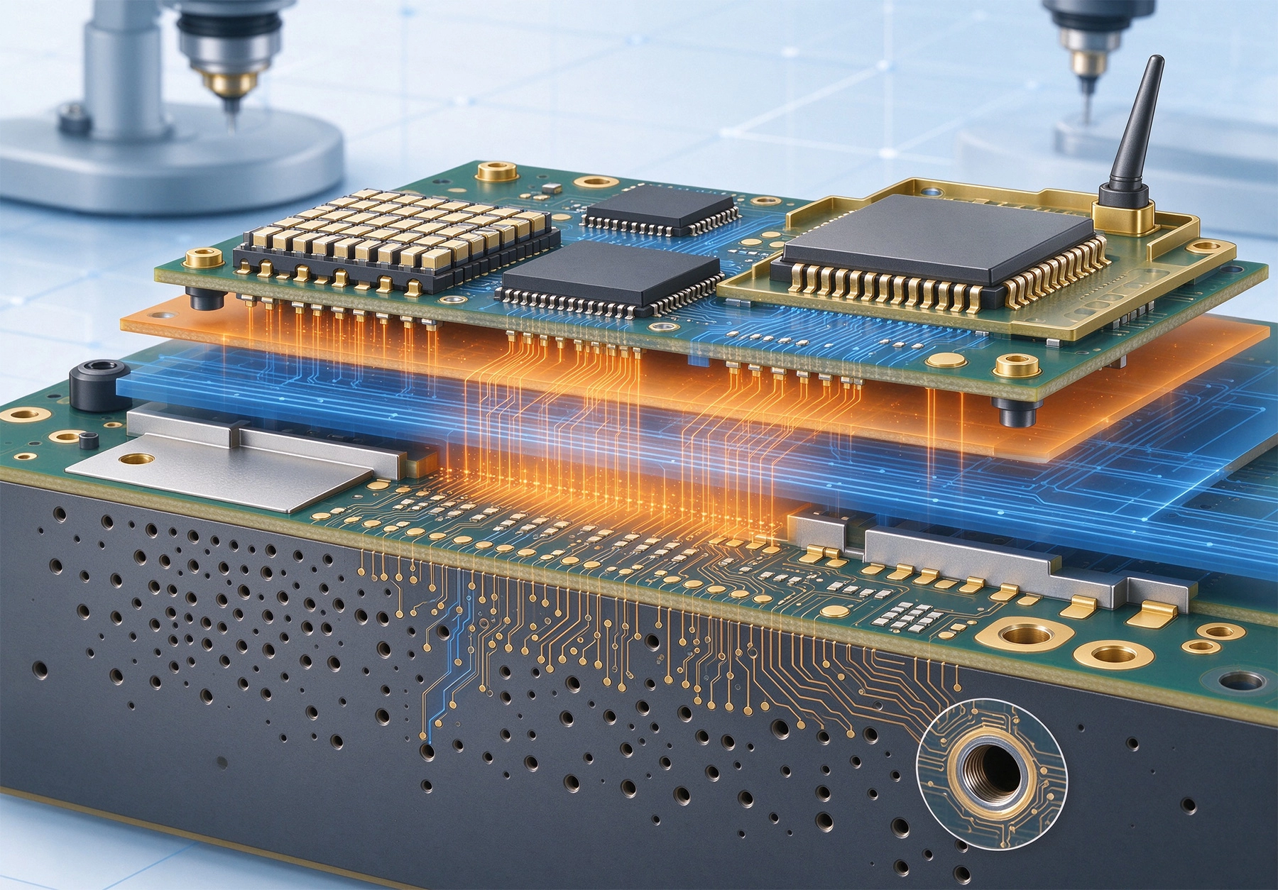
The Impact of HDI on LiDAR and Radar Sensor PerformanceOctober/15/2026Autonomous driving and advanced driver-assistance systems (ADAS) rely on a continuous stream of high-fidelity sensor data. LiDAR and radar are the two primary perception technologies enabling vehicles to "see" their surroundings, but their performance is only as good as the printed circuit boards ...
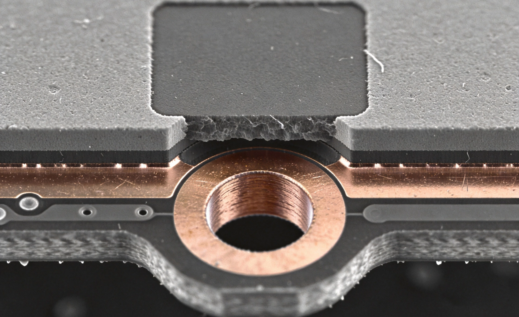
Reliability Challenges of Via-in-Pad Plating Filled (VIPPO) TechnologySeptember/30/2026Via-in-pad is one of those design techniques that looks deceptively simple on a schematic but carries substantial manufacturing complexity underneath. The concept is straightforward: drill a hole at a component pad location, plate it to form an electrical connection to an internal layer, fill it w...
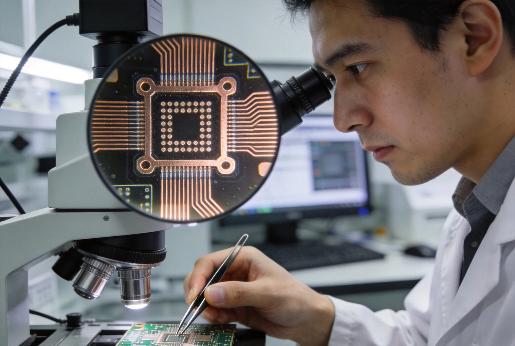
The Role of IPC Standards in HDI PCB Quality AssuranceSeptember/08/2026High Density Interconnect (HDI) PCBs occupy a unique position in the electronics manufacturing landscape: they push the boundaries of what is manufacturable, combining microvia technology, fine-line routing, and advanced materials in structures that are orders of magnitude more complex than the fo...
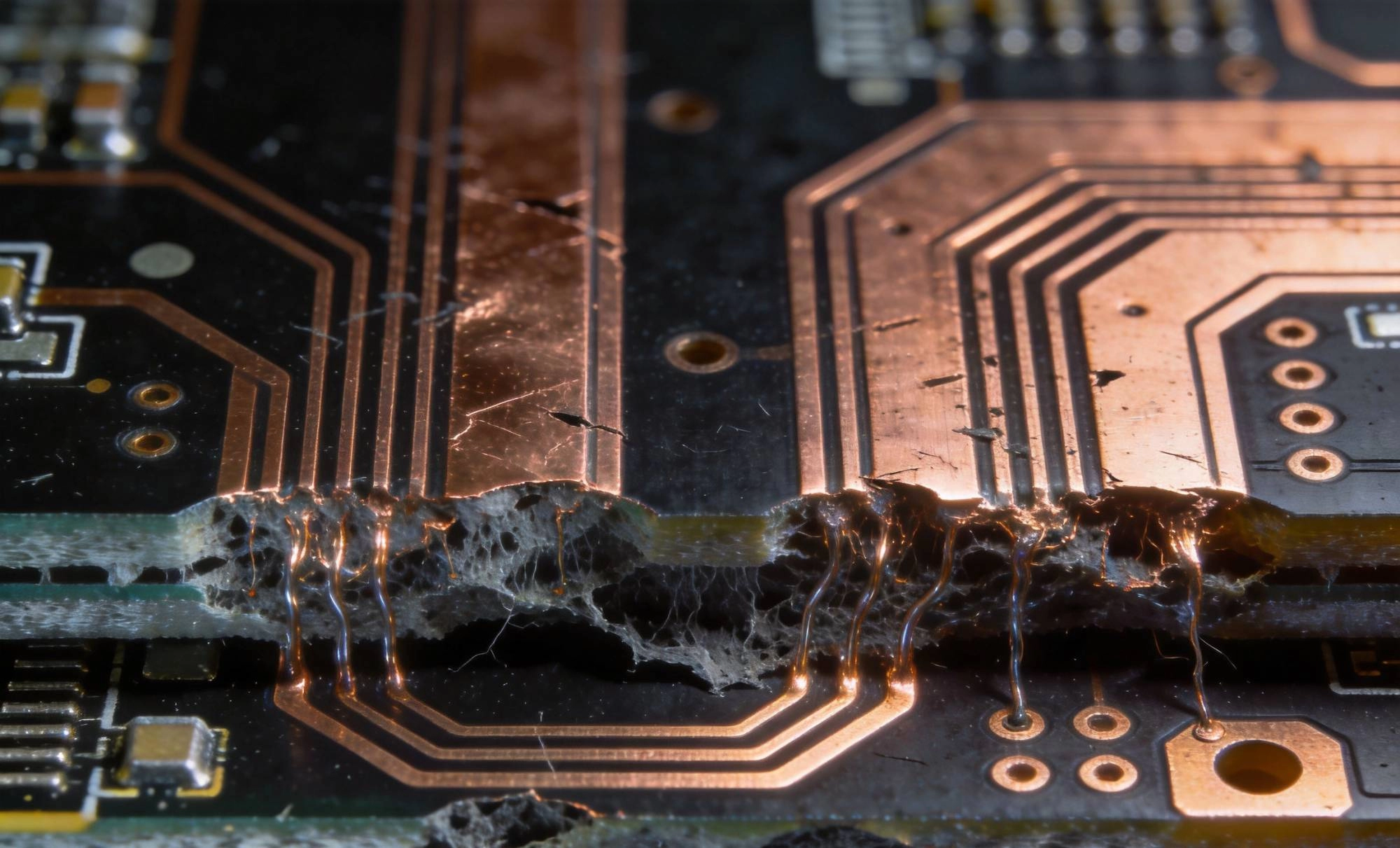
Conductive Anodic Filament (CAF) Resistance in High-Density BoardsJuly/31/2026Conductive Anodic Filament formation represents one of the most insidious failure mechanisms in modern high-density printed circuit boards. Unlike solder joint fractures or component failures that announce themselves with visible symptoms, CAF failures hide within the board laminate, growing gradu...
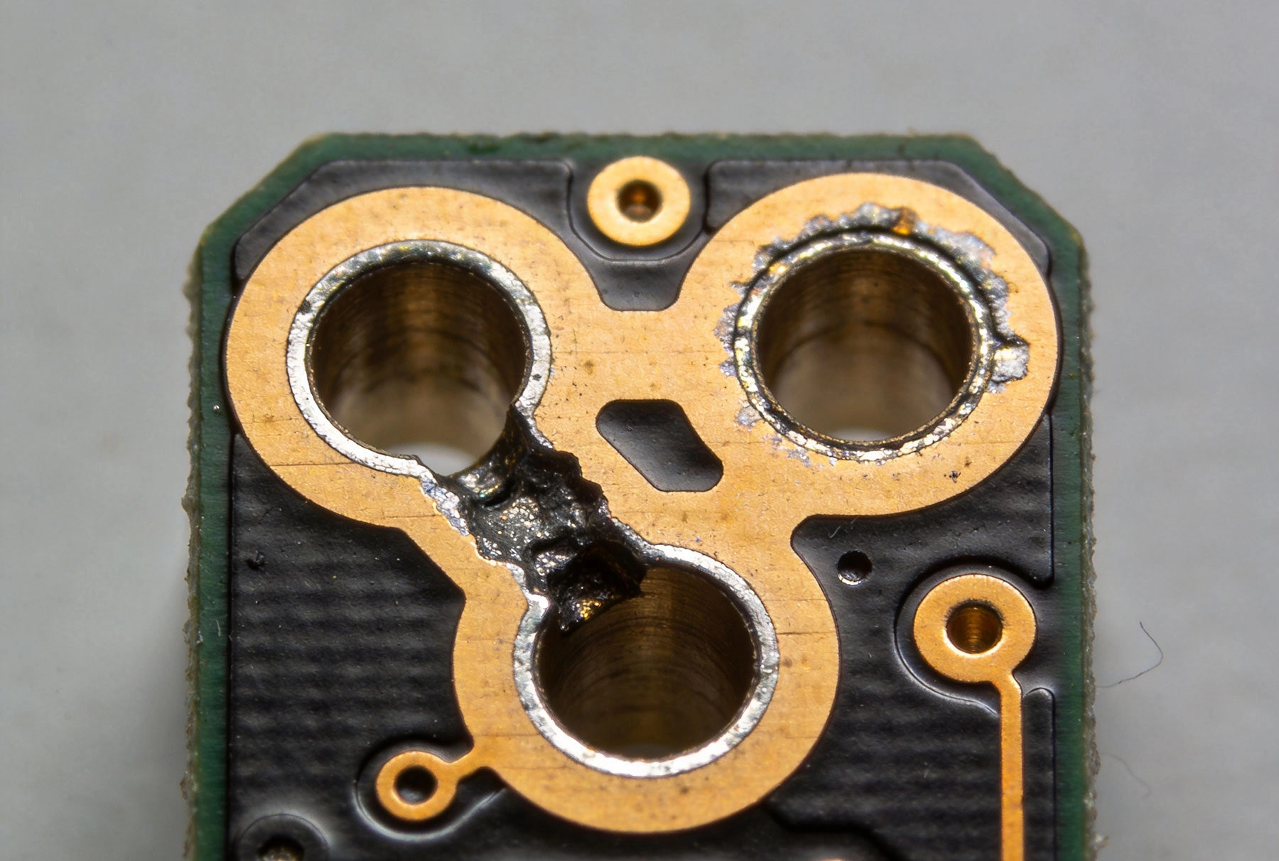
The Impact of Plating Voids on HDI Interconnect ReliabilityJuly/10/2026High-density interconnect (HDI) technology has revolutionized printed circuit board design by enabling unprecedented component density and signal performance. However, the sophisticated microvias and complex plating structures that make HDI possible also introduce specific reliability challenges, ...
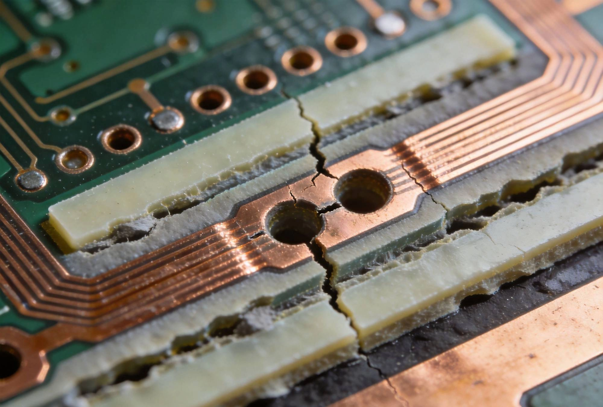
Understanding and Preventing Microvia Cracking in Thermal CyclingJune/12/2026Modern electronic devices demand ever-increasing functionality packed into shrinking form factors. This relentless miniaturization drives the adoption of High-Density Interconnect (HDI) printed circuit board technologies, where microvias serve as the critical interconnections enabling complex rout...