Open Nav

Key materials include advanced resin systems like modified epoxy and BT (bismaleimide triazine) resin, which offer excellent heat resistance and laser-drillability for creating precise Microvias. A critical innovation is the use of ultra-low profile (VLP) copper foil. Its exceptionally smooth surface minimizes the Skin Effect, significantly reducing signal attenuation at high frequencies. For flexible Hdi Applications, polyimide (PI) is favored for its durability and ability to withstand repeated bending. Additionally, advanced build-up films, such as ABF (Ajinomoto Build-up Film), are essential for achieving the fine line widths and high-density layering required in modern Compact Electronics like smartphones and Wearables.
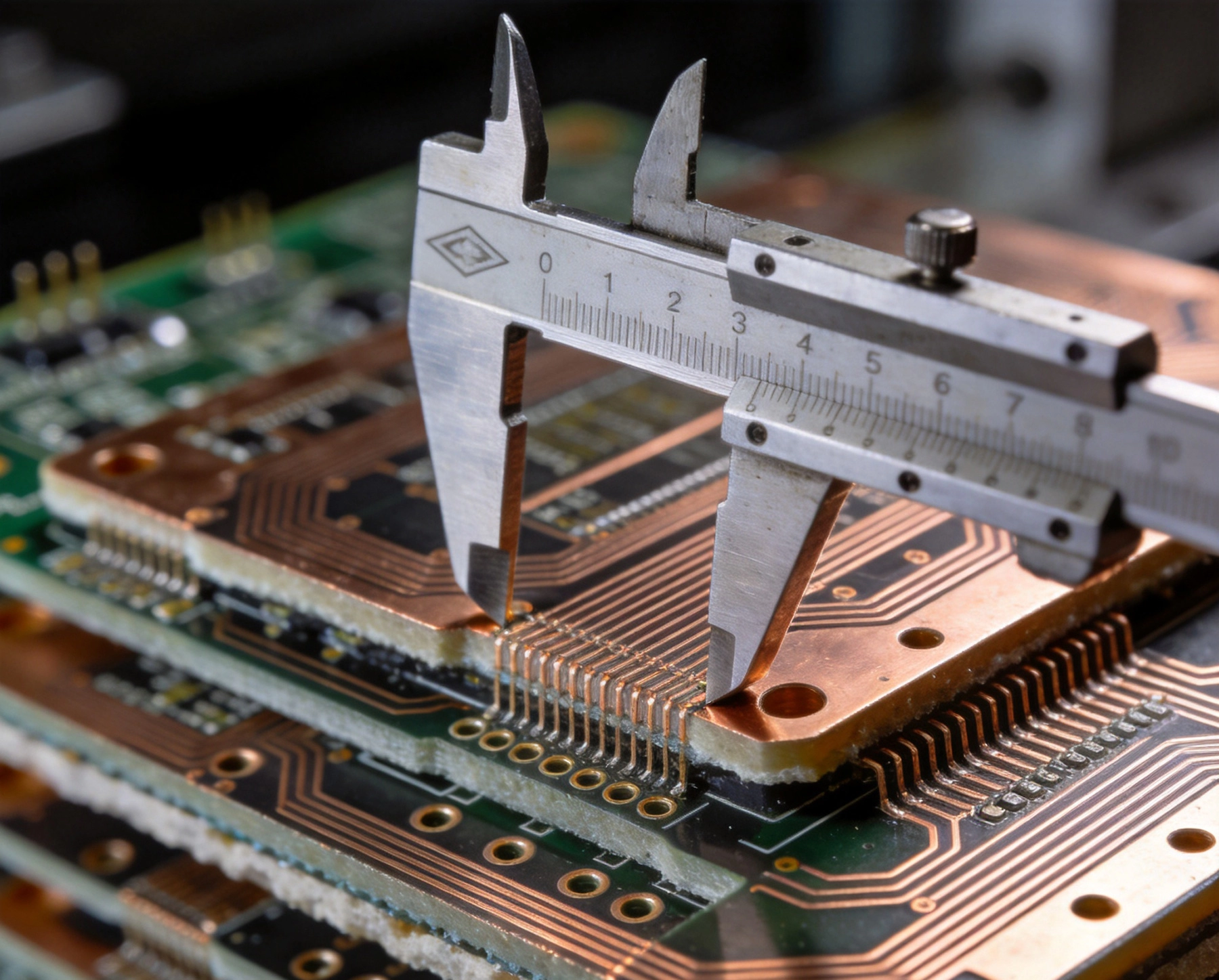
Managing Layer-to-Layer Registration Accuracy in Multilayer HDIOctober/09/2026Registration accuracy—the alignment between layers in a multilayer PCB—doesn't get much attention until it causes problems. And in HDI designs, it causes problems more often than in conventional multilayer boards. The combination of fine features, microvias, and sequential lamination creates align...
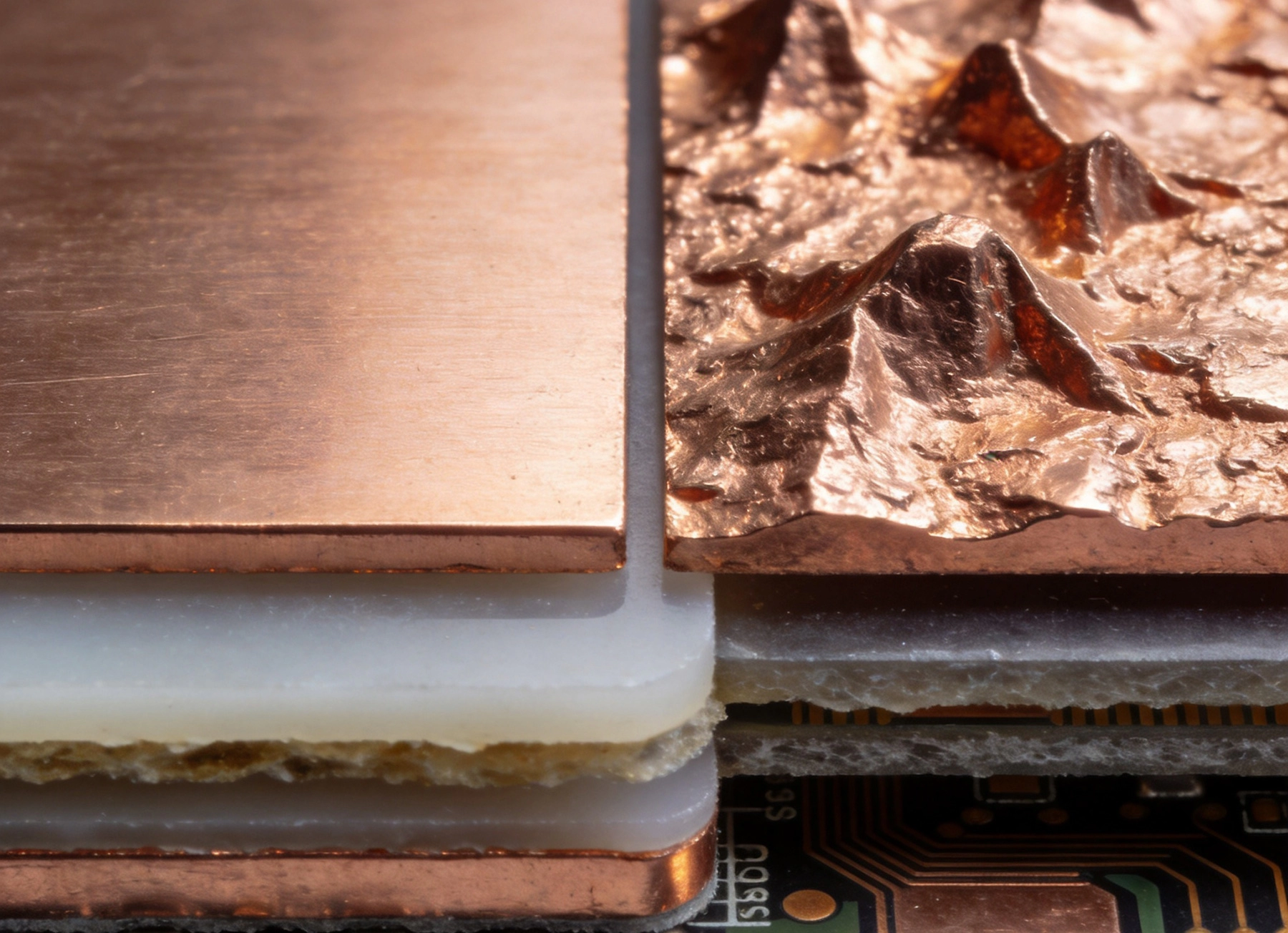
Understanding the Role of Copper Foil Roughness in Signal IntegritySeptember/23/2026Signal integrity engineers spend considerable effort on trace geometry, impedance control, and crosstalk management. Yet one factor often receives insufficient attention until problems emerge in production or field operation: copper foil surface roughness. At low frequencies, the microscopic textu...
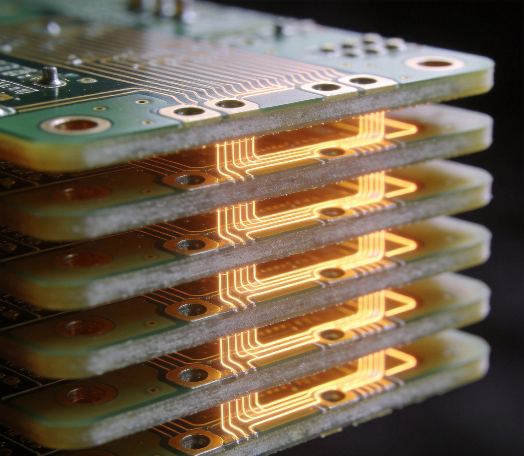
Why Low Loss Materials are Critical for High-Speed HDI DesignsSeptember/01/2026High-density interconnect (HDI) designs enabling 5G communications, high-speed data centers, and advanced automotive radar require printed circuit boards that preserve signal integrity across demanding frequency ranges. Standard FR4 laminates, adequate for legacy applications, introduce excessive ...
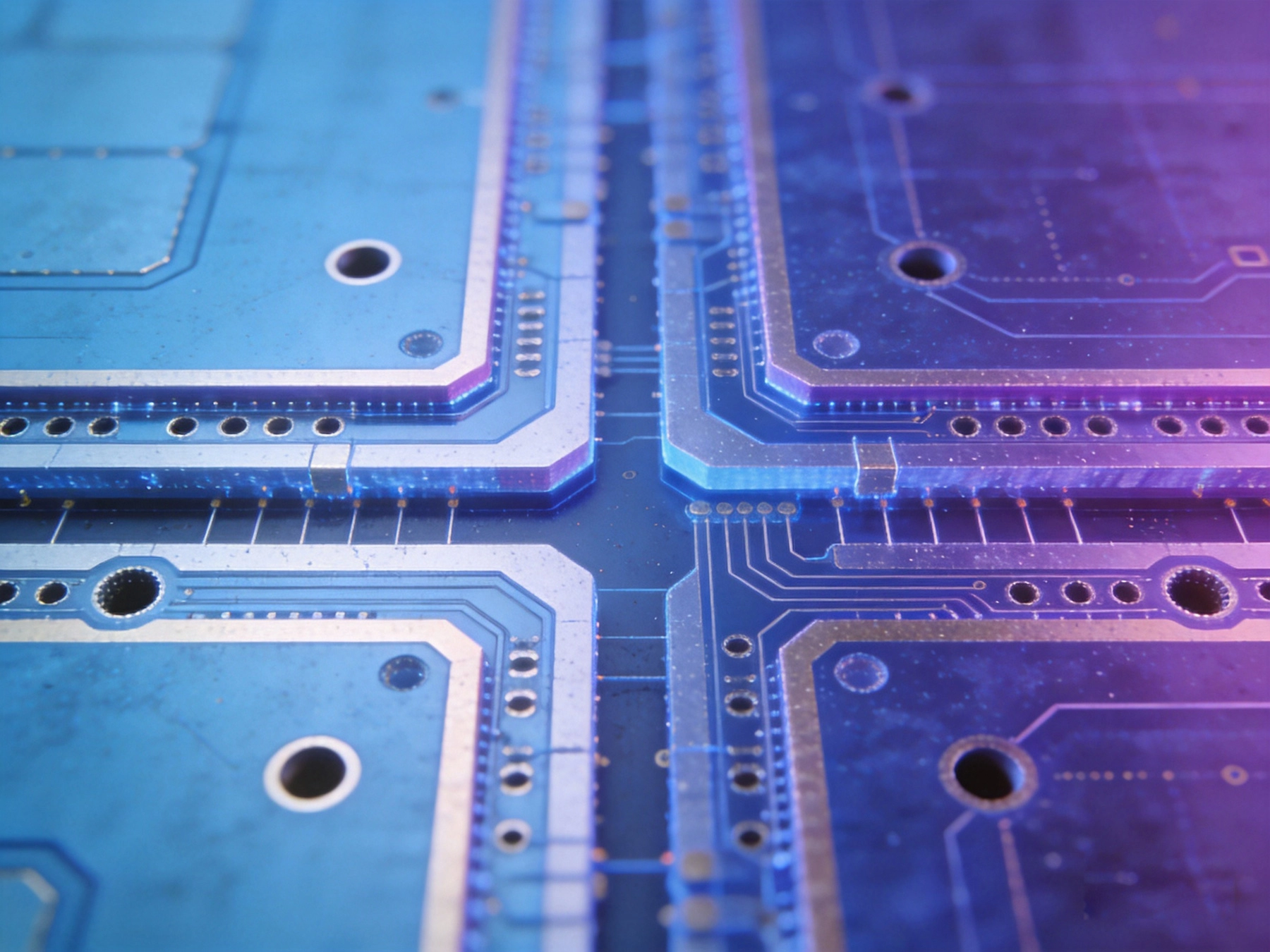
An Introduction to ABF (Ajinomoto Build-up Film) for Advanced HDIJuly/27/2026High Density Interconnect (HDI) technology has become the backbone of modern electronics, enabling the miniaturization that drives smartphones, wearable devices, and high-performance computing systems. At the heart of many advanced HDI constructions lies a specialized material called ABF—Ajinomoto...
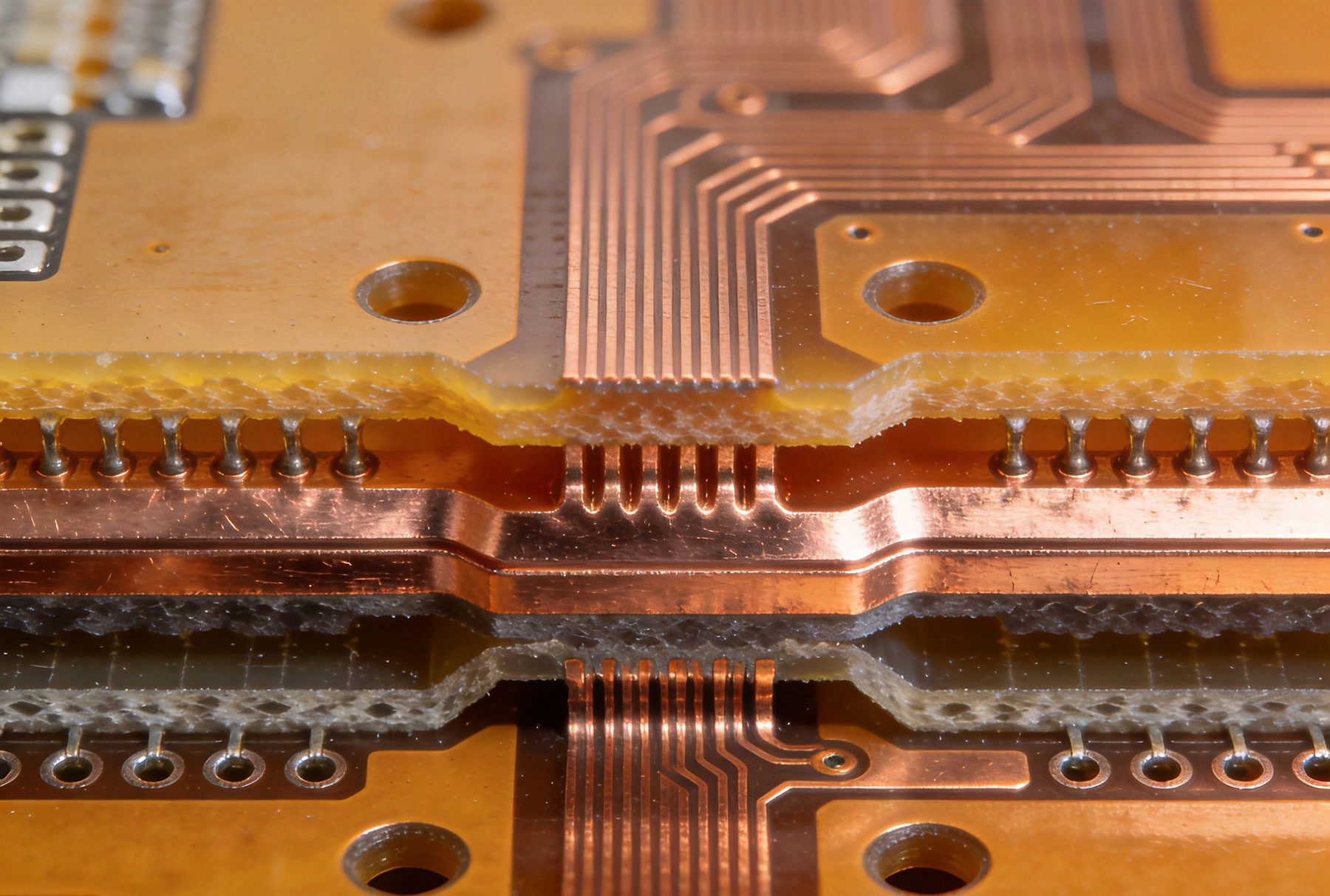
FR-4 vs. High-Tg Materials: What Works Best for HDI Applications?July/07/2026High-density interconnect (HDI) printed circuit boards sit at the heart of virtually every smartphone, tablet, and advanced medical device produced today. The technology enables miniaturization at a scale that would have seemed impossible two decades ago—hundreds of components packed into spaces m...
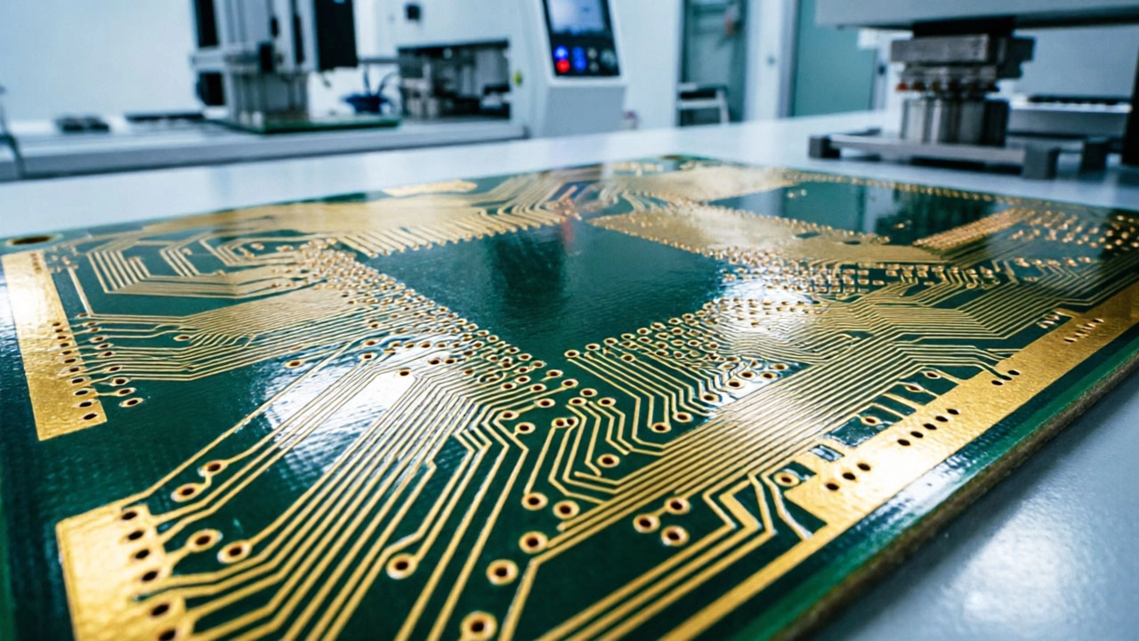
Selecting the Right Dielectric Materials for High-Performance HDI PCBsJune/05/2026High-Density Interconnect (HDI) technology has revolutionized modern electronics, allowing for smaller form factors and higher functionality in devices ranging from smartphones to aerospace avionics. However, as trace widths shrink and signal frequencies rise into the gigahertz range, the choice o...
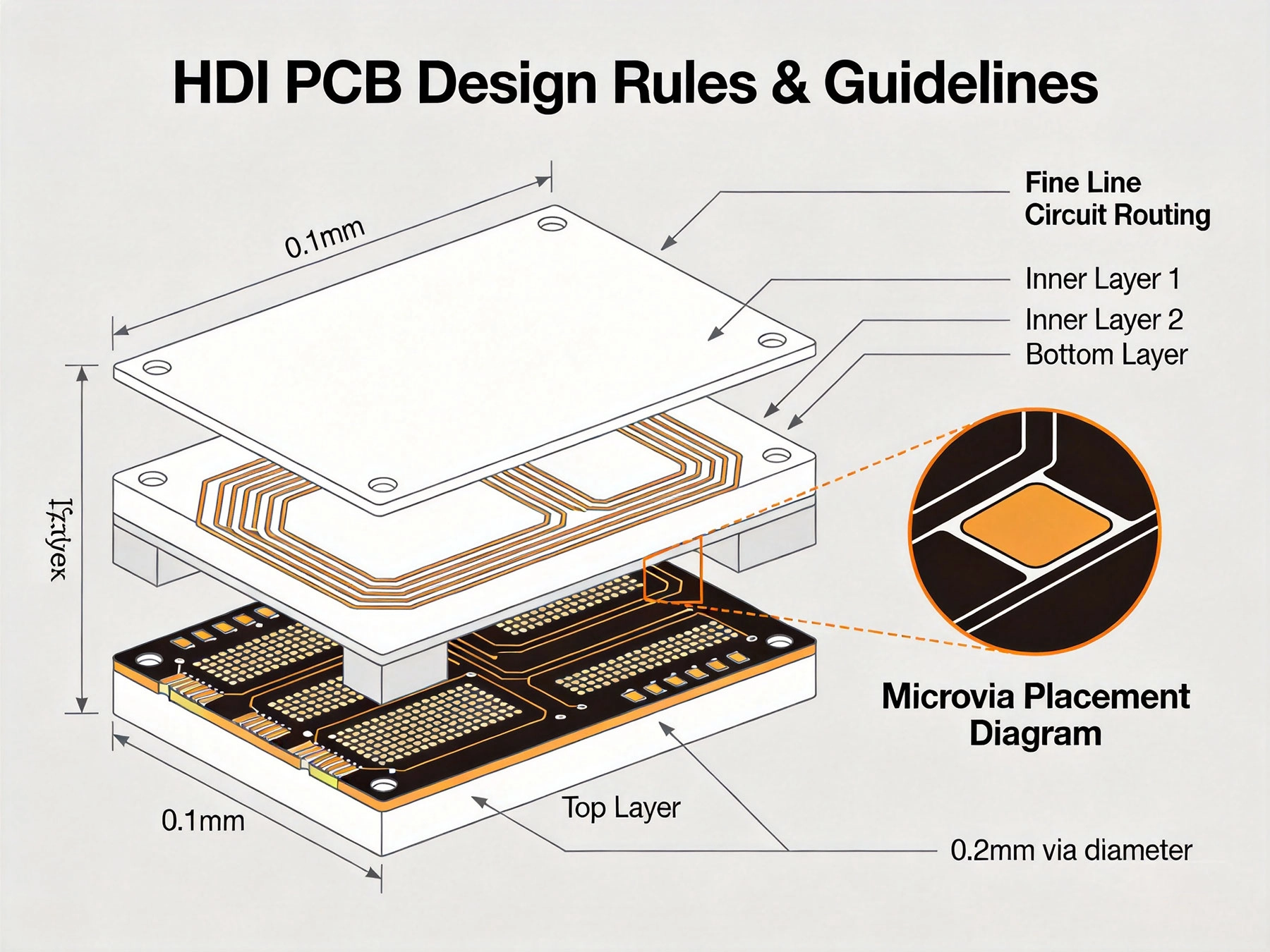
Essential HDI PCB Design Rules for Beginners and ExpertsMay/28/2026Designing an HDI PCB is fundamentally different from designing a conventional multilayer board. The rules you learned for standard PCB layout — things like trace widths, via sizes, and clearance requirements — don't always apply when you're working with 50-micron traces, laser-drilled microvias, a...
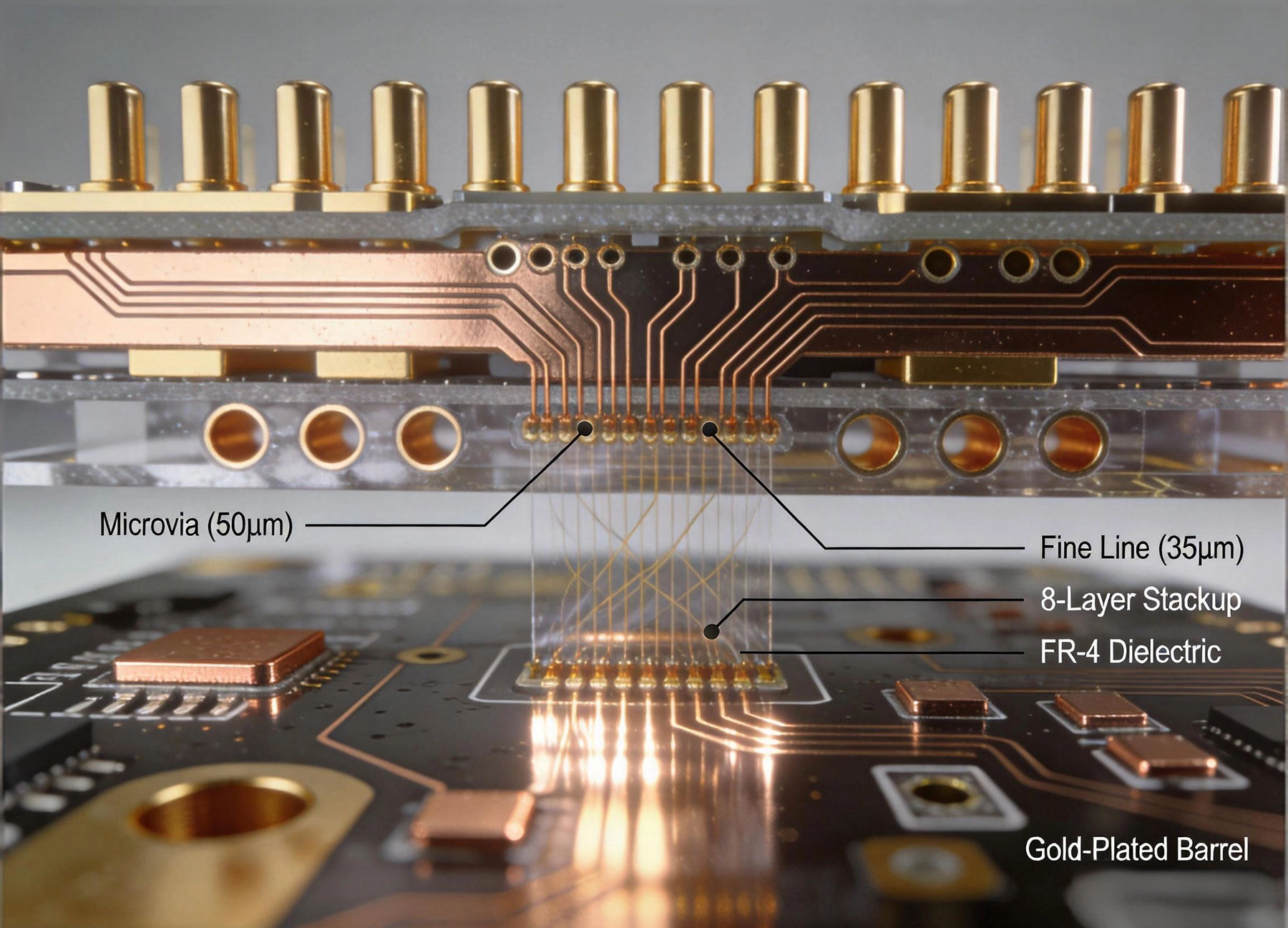
What is High Density Interconnect (HDI) PCB?May/28/2026If you've been working with modern electronics, you've probably heard the term HDI PCB thrown around a lot. But what exactly does it mean, and why is it becoming so important in today's compact devices? In this guide, we'll break down everything about High Density Interconnect (HDI) PCB — from wha...