
By utilizing Microvias, blind and Buried Vias, and fine-line routing, a High Density Interconnect PCB allows for significantly higher component density compared to traditional boards. This is essential for smartphones, tablets, smartwatches, and compact Iot Sensors, where every millimeter of space is valuable. Beyond Miniaturization, these boards enhance electrical performance by shortening signal paths, which reduces power consumption and improves battery life. This makes the High Density Interconnect PCB the perfect solution for delivering high-speed, energy-efficient, and feature-rich experiences in today's connected world.
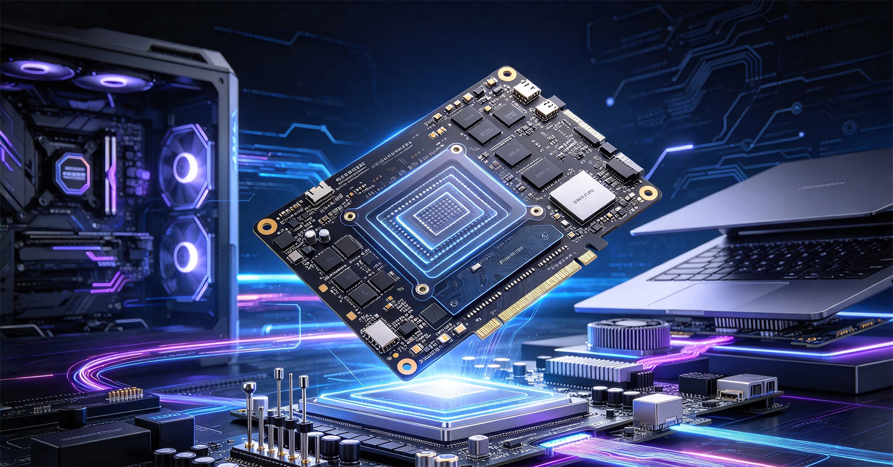
HDI Solutions for High-Performance Gaming Consoles and Laptops October/10/2026 Modern gaming consoles and laptops are pushing hardware limits harder than ever. Faster GPUs, higher memory bandwidth, PCIe 5.0 interfaces, and compact thermal designs all demand more from the printed circuit board. That is why HDI solutions for high-performance gaming consoles and laptops have be...
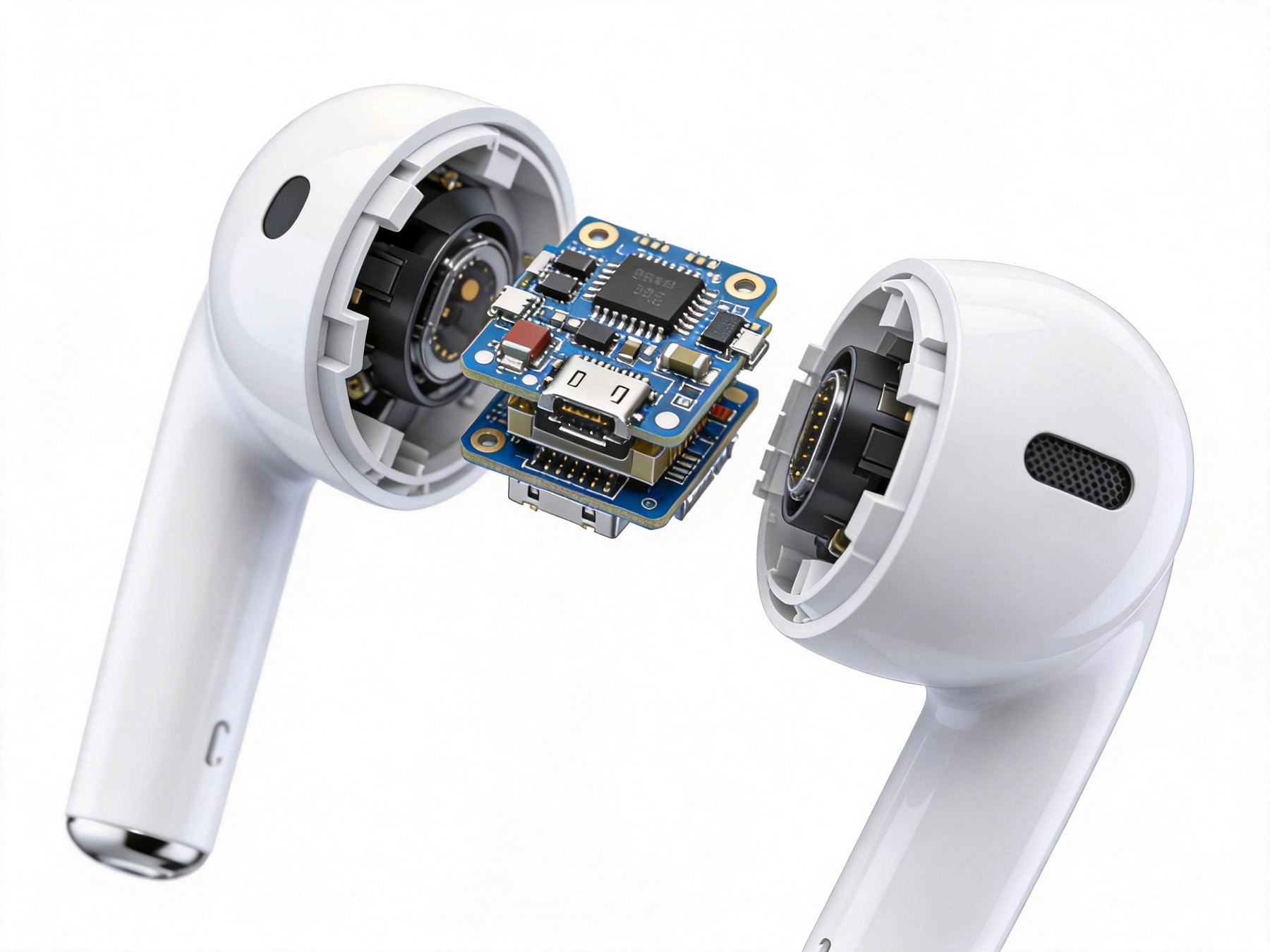
Enabling Compact Designs in True Wireless Stereo (TWS) Earbuds August/06/2026 The True Wireless Stereo earbud market has undergone a remarkable transformation in recent years. What began as relatively large devices with questionable comfort has evolved into sleek, pocket-sized powerhouses that fit virtually imperceptibly in the ear canal. This miniaturization wasn't acciden...