Open Nav

Our tailored HDI PCB Solutions cater to diverse, high-demand sectors. We provide the High Density Interconnect PCB for Energy & Power Electronics to handle high-current loads, and the High Density Interconnect PCB for Automotive & EV Systems for robust Vehicle Electronics. For critical infrastructure, our High Density Interconnect PCB for Telecom 5G & High-speed Computing ensures rapid data transmission. Furthermore, we deliver the High Density Interconnect PCB for Industrial & Automation, the High Density Interconnect PCB for Medical & Healthcare Devices, and the High Density Interconnect PCB for Aerospace, Defense & Avionics, powering innovation across the globe.
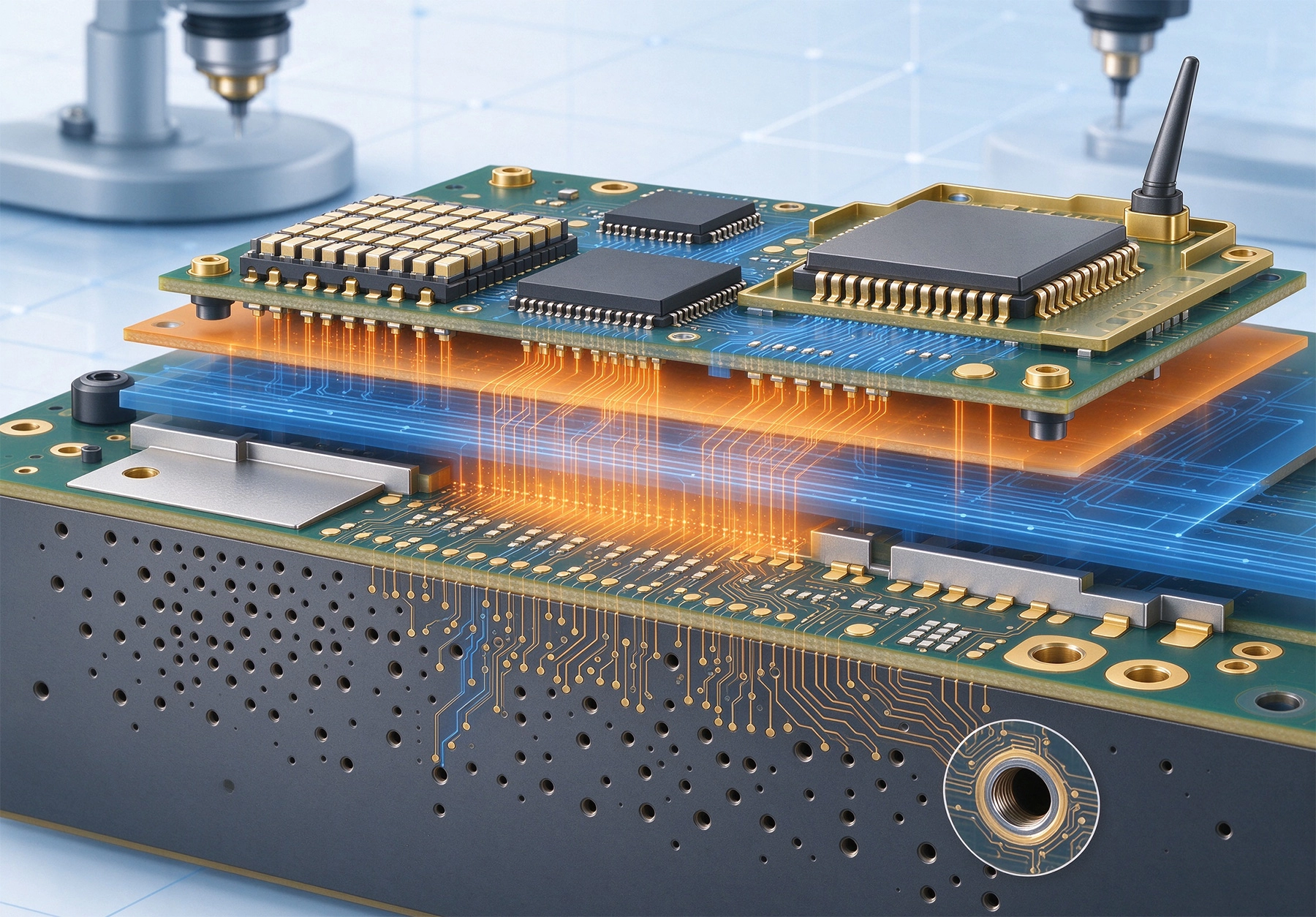
The Impact of HDI on LiDAR and Radar Sensor PerformanceOctober/15/2026Autonomous driving and advanced driver-assistance systems (ADAS) rely on a continuous stream of high-fidelity sensor data. LiDAR and radar are the two primary perception technologies enabling vehicles to "see" their surroundings, but their performance is only as good as the printed circuit boards ...
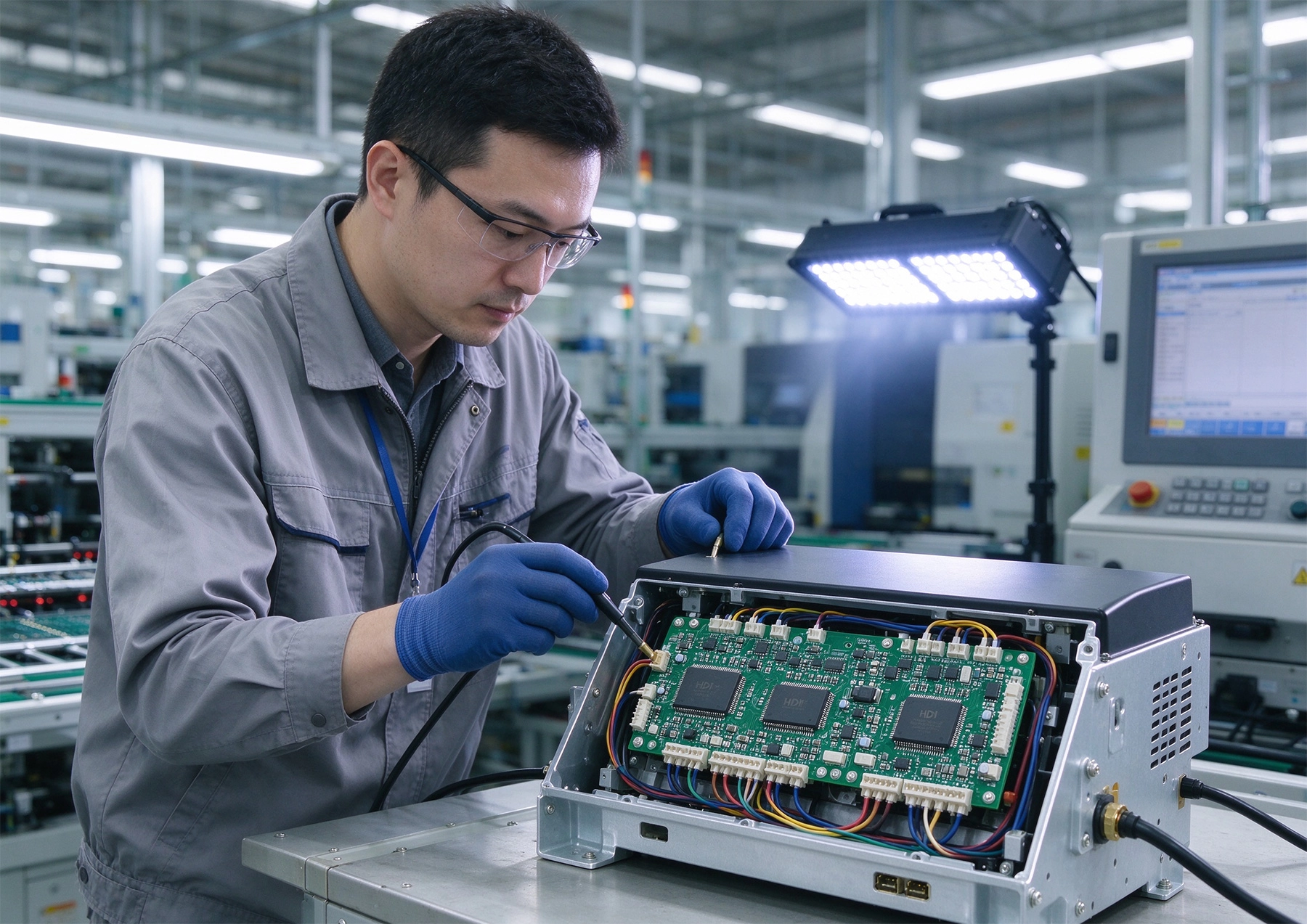
Using HDI Technology in Solar Inverters and ConvertersOctober/14/2026Solar inverters and converters are undergoing a significant transformation. As photovoltaic systems become more powerful, more compact, and more intelligent, the printed circuit boards inside them must handle higher switching frequencies, tighter thermal management, and greater functional density....
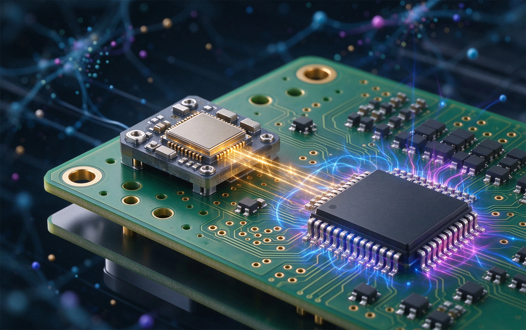
Why IoT Sensors Rely on High-Density Interconnect TechnologyOctober/13/2026Modern IoT sensors are no longer simple devices that read temperature, pressure, or motion and send data through a basic interface. Today’s sensors combine analog front ends, microcontrollers, wireless modules, power management, MEMS structures, and sometimes edge AI processing in extremely small ...
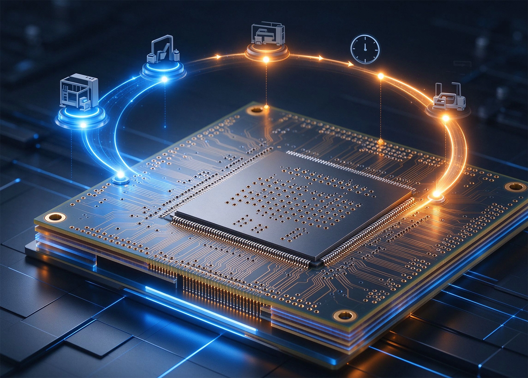
What is the Lead Time for Manufacturing Custom HDI Boards?October/12/2026High-Density Interconnect (HDI) printed circuit boards represent the cutting edge of PCB manufacturing, enabling finer trace widths, smaller vias, and higher component densities than conventional multilayer boards. But with this complexity comes a critical question for every engineer and procureme...
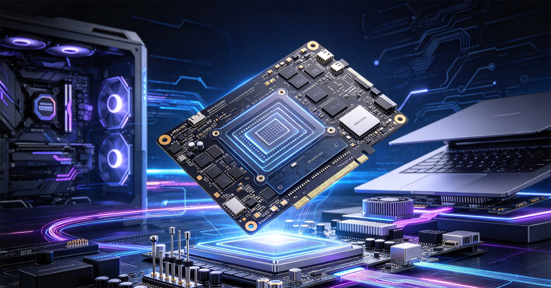
HDI Solutions for High-Performance Gaming Consoles and LaptopsOctober/10/2026Modern gaming consoles and laptops are pushing hardware limits harder than ever. Faster GPUs, higher memory bandwidth, PCIe 5.0 interfaces, and compact thermal designs all demand more from the printed circuit board. That is why HDI solutions for high-performance gaming consoles and laptops have be...
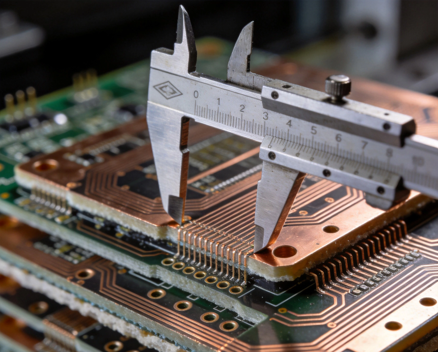
Managing Layer-to-Layer Registration Accuracy in Multilayer HDIOctober/09/2026Registration accuracy—the alignment between layers in a multilayer PCB—doesn't get much attention until it causes problems. And in HDI designs, it causes problems more often than in conventional multilayer boards. The combination of fine features, microvias, and sequential lamination creates align...
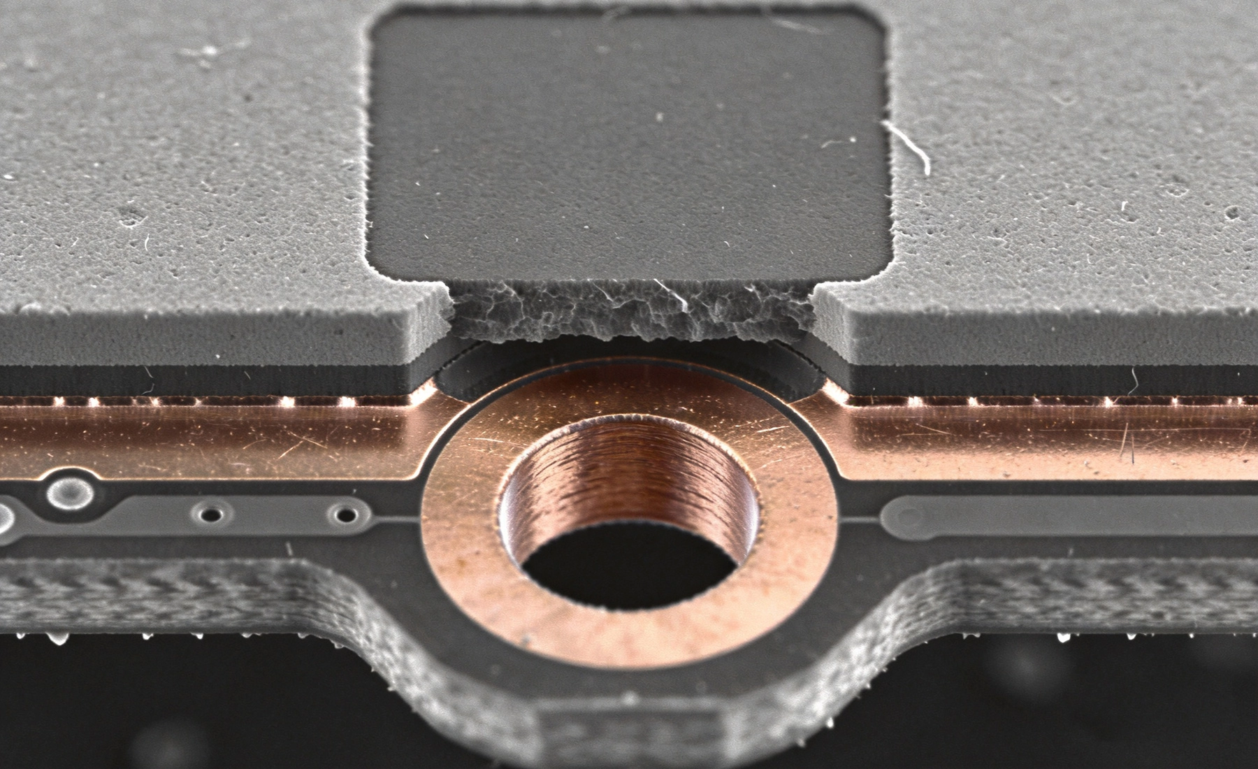
Reliability Challenges of Via-in-Pad Plating Filled (VIPPO) TechnologySeptember/30/2026Via-in-pad is one of those design techniques that looks deceptively simple on a schematic but carries substantial manufacturing complexity underneath. The concept is straightforward: drill a hole at a component pad location, plate it to form an electrical connection to an internal layer, fill it w...
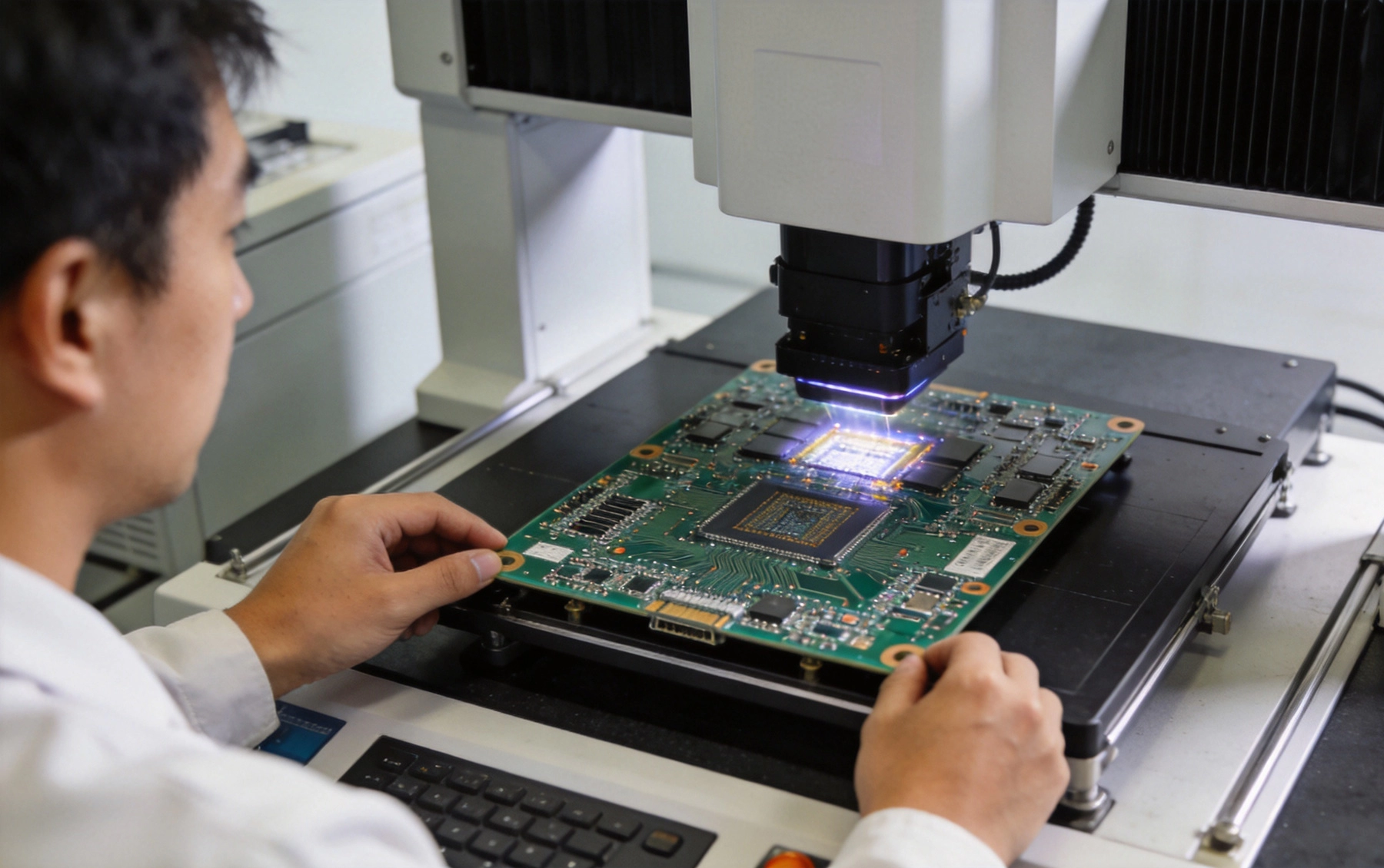
Non-Destructive Testing Techniques for Multilayer HDI PCBsSeptember/29/2026Multilayer High-Density Interconnect (HDI) PCBs form the foundation of modern compact, high-performance electronics including smartphones, medical implants, aerospace systems, and automotive advanced driver assistance systems. With trace widths as small as 25μm, microvias (blind, buried, and stack...
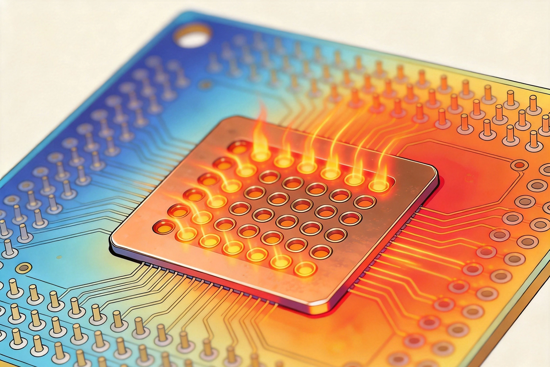
The Impact of Via-in-Pad on Thermal Performance and ReliabilitySeptember/26/2026Via-in-pad — placing a via directly within a component land pad rather than beside it — is one of the most consequential design decisions in modern PCB layout. It affects thermal performance, solder joint integrity, manufacturing cost, and long-term reliability in ways that are not always obvious ...
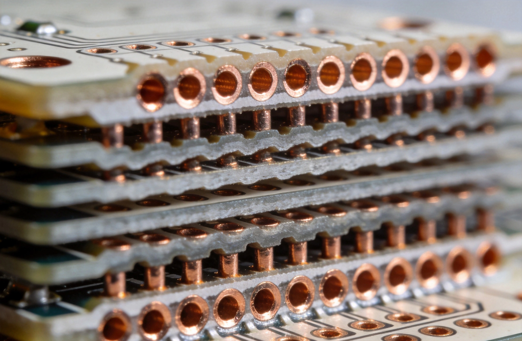
The Art of Microvia Placement: Staggered vs. Stacked ViasSeptember/24/2026As electronics continue their relentless march toward miniaturization, high-density interconnect (HDI) technology has become standard practice rather than exotic exception. And at the heart of every HDI design lies the microvia—those laser-drilled, small-diameter vias that make the interlayer conn...
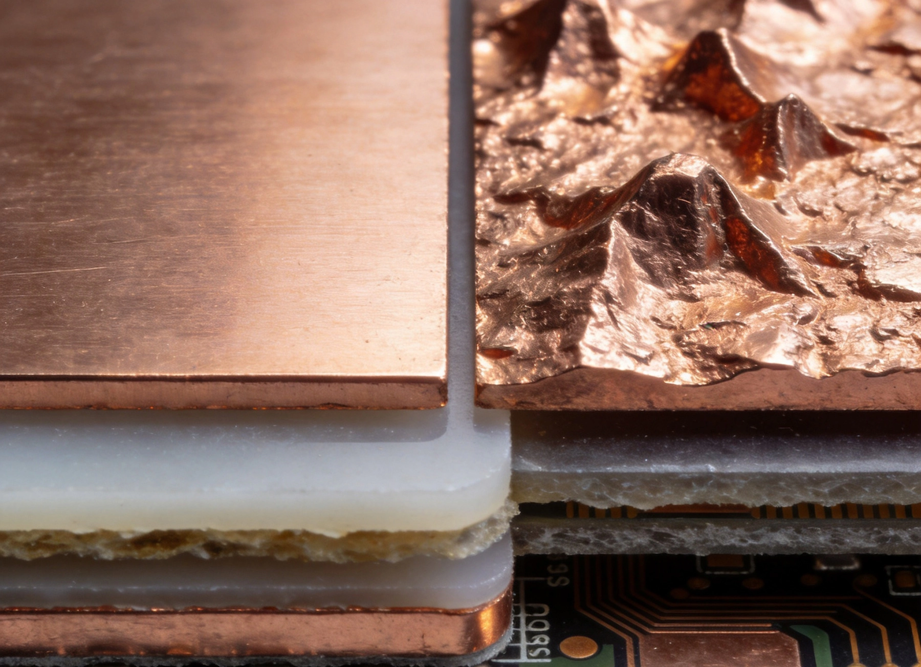
Understanding the Role of Copper Foil Roughness in Signal IntegritySeptember/23/2026Signal integrity engineers spend considerable effort on trace geometry, impedance control, and crosstalk management. Yet one factor often receives insufficient attention until problems emerge in production or field operation: copper foil surface roughness. At low frequencies, the microscopic textu...
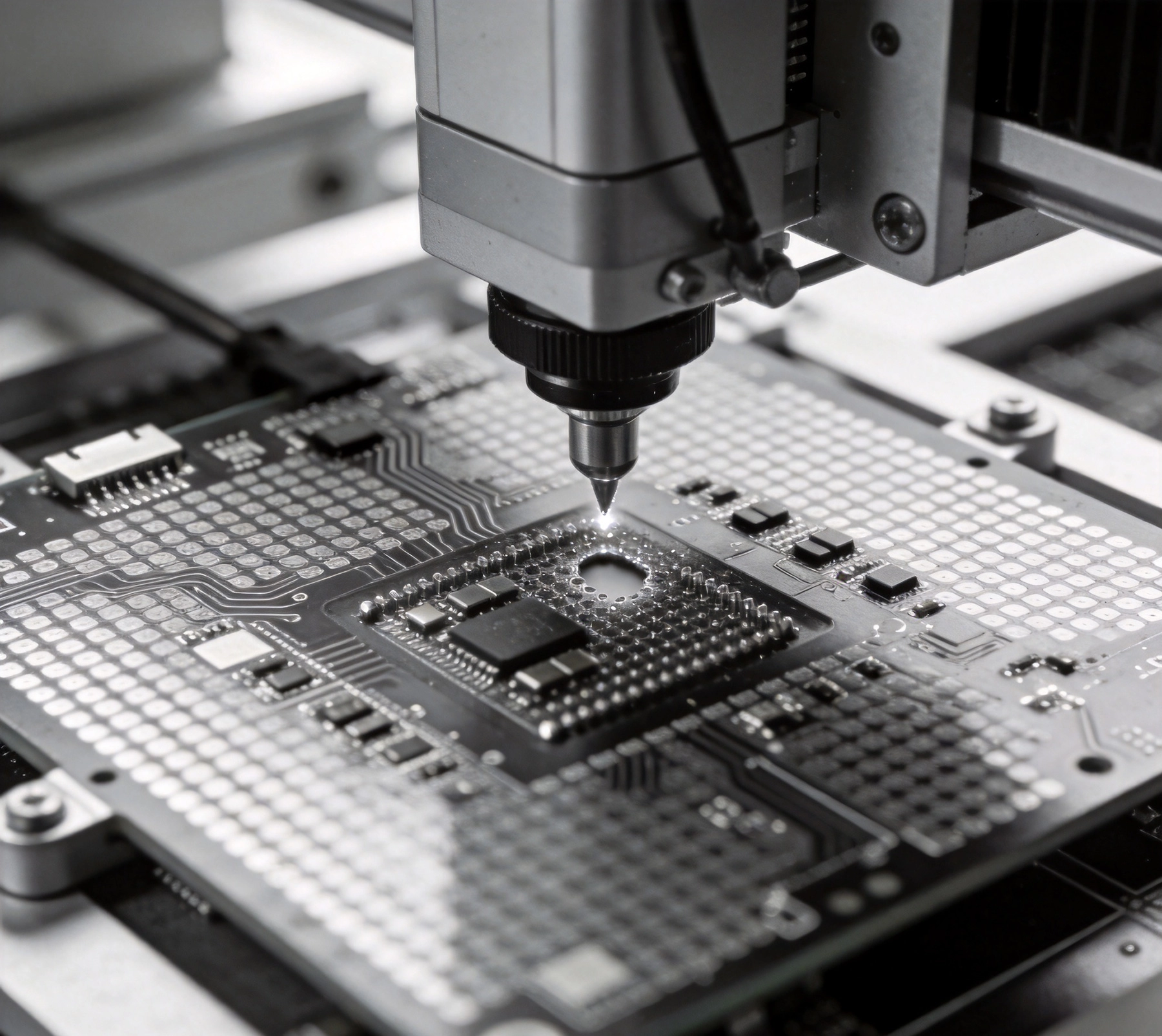
Overcoming Common Manufacturing Defects in High-Density InterconnectsSeptember/21/2026 High-density interconnect (HDI) PCBs have transformed electronics manufacturing by enabling dramatically smaller, lighter, and more capable devices. From smartphones to medical implants, HDI technology makes possible what was impossible with traditional board designs. Yet this miniaturization co...