
Modern IoT sensors are no longer simple devices that read temperature, pressure, or motion and send data through a basic interface. Today’s sensors combine analog front ends, microcontrollers, wireless modules, power management, MEMS structures, and sometimes edge AI processing in extremely small packages. High-density Interconnect, or HDI, technology makes this level of integration possible by allowing more circuitry, shorter signal paths, and finer routing within limited board space.
For IoT designers, HDI is not just a way to shrink a PCB. It is an enabling technology that supports Miniaturization, improved electrical performance, better power efficiency, higher reliability, and more flexible mechanical packaging. As IoT devices move into wearables, medical patches, smart home sensors, industrial monitoring nodes, and automotive systems, HDI becomes increasingly important.
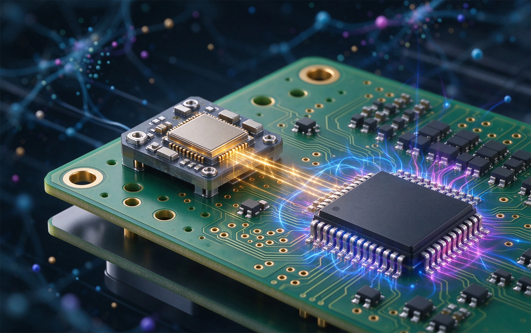
High-density Interconnect PCBs use finer lines and spaces, smaller vias, higher via density, and advanced layer structures to increase routing density. Compared with conventional multilayer boards, Hdi Boards typically include Microvias, Blind Vias, Buried Vias, and stacked or staggered via structures. These features allow signals to move between layers over shorter distances and with less占用 of routing space.
Common HDI structures include:
These structures are especially useful when an IoT sensor uses fine-pitch components such as QFNs, WLCSPs, BGAs, or advanced MEMS packages.
Many IoT sensors must fit into spaces where conventional PCBs cannot. Wearable health monitors, smart rings, hearing aids, environmental sensors, and industrial condition-monitoring nodes all benefit from smaller form factors. A smaller device can be lighter, less intrusive, easier to install, and more acceptable to end users.
Hdi Technology reduces board area by allowing components to be placed closer together and by routing traces through microvias instead of long surface traces. This is particularly important for sensor modules that integrate multiple functions. A single compact node may include a MEMS sensor, a wireless radio, an antenna matching network, a battery management IC, and a secure element. Without HDI, these functions might require a larger board or multiple sub-boards.
Miniaturization also enables new product shapes. Flexible-rigid Hdi Boards can fold around mechanical structures, fit inside curved housings, or connect sensors directly to antennas and displays without bulky connectors.
IoT sensors often handle weak analog signals, high-speed digital interfaces, or mixed-signal traffic. MEMS microphones, accelerometers, gyroscopes, biosensors, and radar sensors can generate signals that are sensitive to noise, crosstalk, and parasitic capacitance. Wireless modules operating at 2.4 GHz, 5 GHz, sub-GHz, or higher frequencies also require careful layout.
HDI boards shorten signal paths by moving connections through microvias instead of long traces. Shorter paths reduce parasitic inductance and capacitance, which helps maintain signal quality. For mixed-signal designs, HDI also makes it easier to create dedicated ground returns, shield sensitive traces, and separate analog and digital domains within a small area.
This matters even when data rates are modest. A sensor node may not operate at multi-gigabit speeds, but it may still require clean power distribution, low-noise analog routing, and stable RF performance. HDI structures support these requirements without forcing the board to grow larger.
Most IoT sensors are battery-powered or energy-harvesting devices. Power efficiency determines how long a device can operate, how often it needs maintenance, and whether it can be deployed in remote locations. Hdi Technology contributes to power efficiency in several ways.
Shorter traces reduce resistive loss and switching noise. Compact power loops around DC-DC converters and RF power amplifiers reduce electromagnetic interference and improve conversion efficiency. Dense ground via arrays help remove heat from small components, which can improve stability and reduce performance drift. Better power delivery also allows designers to use smaller passive components without sacrificing reliability.
In wearable and medical sensors, these benefits are especially valuable. A small reduction in power consumption can extend battery life from weeks to months, or make energy harvesting feasible for the first time.
Modern sensors use increasingly advanced packages. System-in-package modules, wafer-level chip-scale packages, flip-chip devices, and fine-pitch BGAs all require dense interconnects. Conventional through-hole vias and wide trace spacing cannot always reach the necessary pad density.
Microvias allow designers to fan out signals from fine-pitch devices without adding excessive layers. Stacked or staggered microvias provide vertical interconnection while keeping the outer layers available for components and antennas. This is critical for IoT modules that must combine sensing, processing, connectivity, and security in one compact assembly.
HDI also supports integration of passive components into or under the board surface in some advanced designs. While not every IoT sensor uses embedded passives, the same manufacturing discipline that enables HDI often enables more compact component placement and better space utilization.
IoT sensors are deployed in factories, vehicles, outdoor infrastructure, agricultural fields, and medical environments. They may experience vibration, thermal cycling, humidity, dust, and mechanical shock. HDI boards can improve reliability when designed correctly.
Blind and buried vias reduce the number of long through-hole vias, which can lower stress points in the board. Microvias with proper aspect ratios and plating can provide reliable interlayer connections for high-density designs. Shorter interconnects also reduce mechanical leverage on solder joints, which may help improve resistance to vibration and shock.
However, Hdi Reliability depends on good design and process control. Stacked Microvias, high aspect ratios, and complex via structures must be validated for the expected thermal and mechanical environment. For automotive, industrial, or medical sensors, designers should work closely with fabricators to confirm via fill materials, plating thickness, reliability testing, and inspection methods.
HDI technology offers clear advantages, but it also increases manufacturing complexity. Laser-drilled microvias, Via Filling, Sequential Lamination, and fine-line imaging require more process steps than conventional PCBs. This can affect cost, lead time, and yield.
For IoT products, the key is to match HDI complexity to product requirements. Not every sensor node needs Any-layer Hdi. Many designs can achieve sufficient density with one or two Microvia layers, blind vias, and careful component placement. Overdesigning the HDI structure can add cost without meaningful benefit.
Important manufacturing considerations include:
Early collaboration with the PCB fabricator and PCBA supplier helps avoid redesigns. Decisions about via structure, layer count, and material selection should be made during schematic and stackup planning, not after layout is complete.
HDI boards usually cost more per unit than conventional boards. For high-volume, cost-sensitive IoT sensors, this can seem like a disadvantage. However, HDI should be evaluated as a system-level decision rather than a bare PCB cost item.
HDI can reduce total system cost by enabling smaller enclosures, fewer mechanical components, simpler assembly, lower shipping weight, longer battery life, and higher functional integration. In medical wearables or industrial sensors, the cost of a larger device may exceed the additional PCB expense. In consumer IoT products, miniaturization can directly affect user adoption.
The most effective approach is to use HDI where it creates measurable value. Critical RF sections, fine-pitch processors, dense sensor arrays, and space-constrained wearables benefit most. Simpler sensor nodes with low pin-count devices may not need advanced HDI structures.
Several trends will increase the reliance of IoT sensors on HDI technology. Edge AI requires more processing power inside small devices. Multi-Sensor Fusion combines vision, audio, motion, environmental, and biometric data in a single node. Ultra-wideband, Wi-Fi 6/7, Bluetooth Low Energy, and cellular IoT modules continue to shrink while adding functionality. At the same time, batteries are not shrinking at the same rate, so electronics must become more efficient and compact.
Advanced packaging, substrate-like PCBs, and rigid-flex HDI boards will also play larger roles. These technologies blur the boundary between PCB and package, allowing IoT sensors to achieve higher performance without increasing size. As manufacturing capabilities mature, HDI will become more accessible for mid-volume IoT products, not only for premium smartphones and high-end computing devices.
IoT sensors rely on high-density interconnect technology because miniaturization, integration, signal quality, power efficiency, and reliability are no longer optional features. HDI enables designers to pack more functionality into smaller spaces while maintaining clean power delivery, short signal paths, and robust mechanical performance. It also supports advanced components and wireless functions that define modern IoT devices.
The decision to use HDI should be guided by system requirements rather than density alone. When applied correctly, HDI does not just make an IoT sensor smaller. It makes the entire product more capable, more efficient, and more suitable for real-world deployment.
IoT sensors often combine sensing, processing, wireless communication, and power management in very small packages. HDI provides the routing density, short interconnects, and advanced via structures needed for this level of integration.
Yes. Microvias and shorter traces reduce parasitic effects, crosstalk, and loop inductance. This helps analog sensors, RF circuits, and mixed-signal designs maintain better signal quality.
HDI increases PCB cost, but it can reduce total system cost by enabling smaller enclosures, longer battery life, fewer components, and higher integration. The value depends on the application.
Microvias, blind vias, buried vias, fine lines and spaces, and dense ground connections are among the most useful features. They support fine-pitch components, compact layouts, and reliable power distribution.
If the design uses low pin-count components, has generous board space, and does not require high-frequency or high-density routing, a conventional Multilayer Pcb may be more cost-effective.
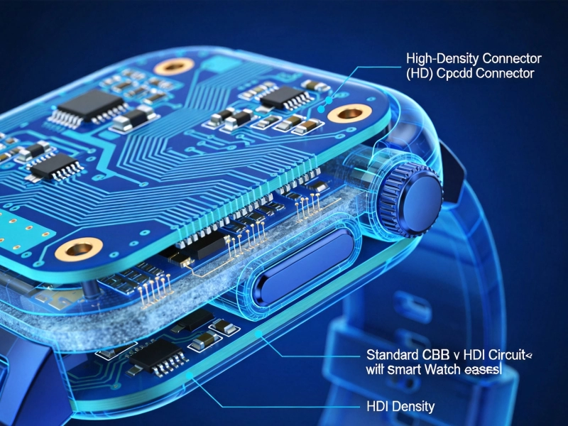
The Role of HDI Technology in Wearable Device MiniaturizationJuly/15/2026
Using HDI Technology in Solar Inverters and ConvertersOctober/14/2026
High-Reliability Standards for HDI in Life-Critical Healthcare EquipmentAugust/11/2026
The Role of HDI PCBs in Miniaturized Implantable Medical DevicesJuly/21/2026
HDI Solutions for Wearable Health Monitors and Diagnostic ToolsSeptember/17/2026
The Impact of Via-in-Pad on Thermal Performance and ReliabilitySeptember/26/2026
How to Use Thermal Simulation Software to Optimize HDI LayoutsJuly/29/2026
What is the Lead Time for Manufacturing Custom HDI Boards?October/12/2026