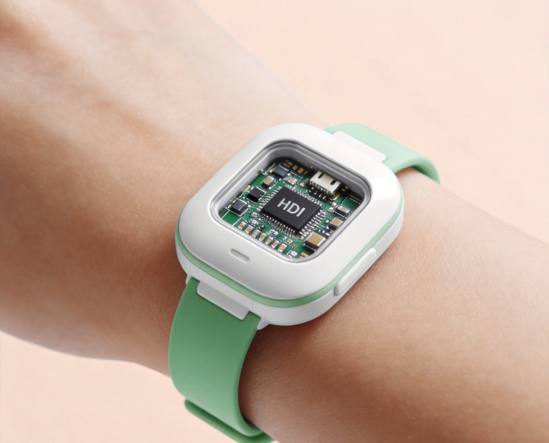
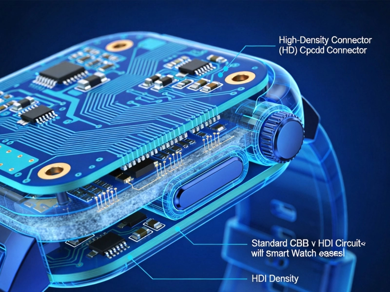
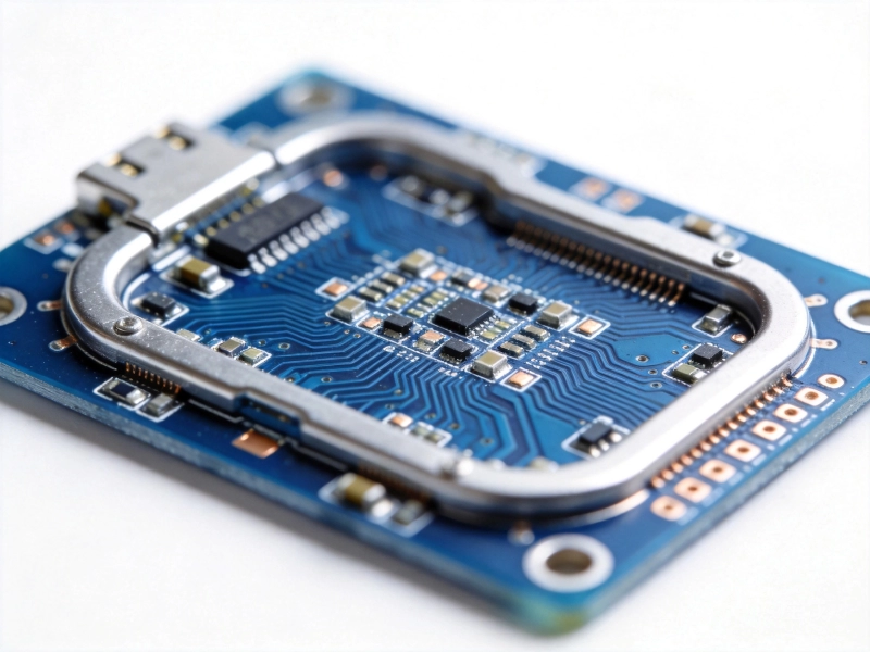
The wearable health technology market is experiencing explosive growth, driven by consumer demand for continuous biometric monitoring and clinician demand for ambulatory diagnostic data. From continuous glucose monitors and cardiac event recorders to pulse oximeters and blood pressure watches, these devices share a common engineering challenge: packing sophisticated sensing, signal processing, wireless communication, and power management into a form factor that patients actually want to wear. High-density Interconnect (HDI) Pcb Technology is the enabling technology that makes this possible—not merely helpful, but genuinely essential. Without HDI, most modern wearable health monitors could not exist in their current form factors. This article examines how HDI solutions address the unique requirements of wearable health monitors and diagnostic tools, from extreme Miniaturization to biocompatiblity, from flexible-rigid construction to medical-grade reliability.

Why Wearable Health Devices Demand HDI
Wearable health monitors impose a set of concurrent constraints that converge on HDI as the only viable PCB construction:
-
Extreme area constraint: A wrist-worn health monitor typically has a PCB area of 200–600 mm². A continuous glucose monitor (CGM) patch has perhaps 100–200 mm². A hearing aid or TWS-style in-ear diagnostic device may have just 40–80 mm². At these scales, every via, every trace, every component pad consumes a precious fraction of the available routing space.
-
High I/O density from SoC integration: Wearable health monitors are built around highly integrated SoCs that combine an application processor, wireless transceiver (BLE or BLE+UWB), sensor interfaces, and analog front-ends on a single die. These SoCs use 0.4 mm pitch WLCSP or BGA packages with 100–400+ connections. Escaping these packages on a conventional PCB would require an impractically large number of layers or board area that exceeds the wearable form factor.
-
Thickness constraint: A wrist-worn device PCB is typically 0.4–0.8 mm thick. A skin-attached patch may need to be 0.2–0.4 mm. Conventional multilayer construction (with through-hole vias penetrating all layers) cannot achieve these thicknesses while maintaining adequate routing density. HDI with Microvias that connect only adjacent layer pairs enables thin constructions with high routing density.
-
Mixed rigid and flexible regions: Many wearable devices require rigid sections for component mounting and flexible sections for ergonomic conformity to the body. Rigid-flex HDI construction integrates both on a single PCB, eliminating inter-board connectors that consume space and reduce reliability.
HDI Construction Types for Wearable Health Monitors
Different wearable form factors favor different HDI construction approaches:
Any-Layer HDI for Wrist-Worn Devices
Smartwatches and health-monitoring watches use Any-layer Hdi construction where Microvias can connect any adjacent layer pair, with Stacked Microvias enabling vertical routing through multiple layers. A typical construction is 1+4+1 (one Microvia layer on each side of a 4-layer FR4 core) or 2+4+2 for more complex designs with higher I/O counts.
The Any-Layer approach is necessary because the SoC escape routing demands Via-in-pad on most BGA pads—placing a Microvia directly beneath each pad rather than routing a short trace to a via outside the pad perimeter. On a 0.4 mm pitch BGA with 0.25 mm pads, there is only 0.15 mm between pads—insufficient for a conventional via even at the smallest drill sizes. Only a 0.1 mm microvia fits within the pad geometry.
Rigid-Flex HDI for Skin-Attached Patches
Continuous glucose monitors, cardiac monitoring patches, and drug delivery devices adhere directly to the skin. The electronics section must be rigid for component mounting, while the "tail" that routes sensor connections, antenna traces, and battery contacts must be flexible to conform to body contours and accommodate movement.
Rigid-flex HDI combines conventional rigid HDI sections (with build-up microvia layers) and polyimide flexible sections (with single- or double-sided copper). The transition between rigid and flex sections—where the build-up layers terminate and the flexible core continues—requires precise manufacturing control. The microvias in the rigid section must not extend into the flex region, and the copper patterns at the rigid-flex boundary must maintain continuity without stress concentrations.
Flexible HDI for In-Ear and Catheter Devices
The most extreme form factor constraints appear in in-ear diagnostic devices (hearing aid-style health monitors, in-ear temperature sensors) and catheter-based diagnostic tools (intravascular ultrasound, endoscopic sensors). These devices require fully flexible HDI constructions where the entire PCB is a thin polyimide substrate with microvias connecting copper layers.
Flexible HDI presents unique Microvia Reliability challenges. The repeated bending that the device experiences in use—whether from ear canal movement or catheter articulation—subjects microvias to mechanical stress that rigid HDI never sees. Copper-filled microvias with enhanced plating (sometimes with nickel barrier layers) are essential for flexible Hdi Reliability in medical applications.
Key Functional Blocks and Their HDI Requirements
Wearable health monitors contain several functional blocks, each with specific PCB requirements that HDI must satisfy.
Biometric Sensor Front-End
The sensor front-end is the defining circuit block of any health monitor. Common sensors and their PCB implications:
-
PPG (Photoplethysmography) for heart rate and SpO2: Requires precise placement of LED emitters (green, red, infrared) and photodiodes with controlled optical geometry. The PCB must include optical barriers—copper walls or trenches between the emitter and detector channels—to prevent optical crosstalk. HDI's fine-line capability (3–4 mil traces) enables the routing density needed for multi-wavelength PPG designs with 2–4 emitter-detector pairs.
-
ECG/ECG analog front-end: Dry electrode or wet electrode ECG requires ultra-low-noise analog routing with guard traces and Differential Pair Routing from the electrode contacts to the AFE IC. HDI enables short, direct routing from electrode pads on the PCB periphery to the AFE, minimizing noise pickup. Via-in-pad at the AFE BGA ensures that the sensitive analog inputs are connected with minimal stub length, reducing parasitic capacitance that limits bandwidth.
-
Accelerometer/gyroscope for activity and fall detection: MEMS inertial sensors use QFN or LGA packages with 0.5 mm pitch. While not requiring HDI for escape routing alone, the overall board density in a wearable makes HDI necessary to route the IMU connections alongside all other circuit blocks.
-
Bioimpedance for body composition and hydration: Bioimpedance measurement uses AC excitation at multiple frequencies (1 kHz to 1 MHz) and requires careful separation of excitation and measurement paths. HDI's ability to create guard traces and ground-plane isolation between adjacent analog channels is critical for measurement accuracy.
Wireless Communication
Every wearable health monitor requires wireless connectivity—to a smartphone gateway, to a clinical monitoring system, or to a cloud analytics platform. The wireless subsystem has specific HDI requirements:
-
BLE antenna integration: The Bluetooth antenna is typically a printed trace antenna (meandered monopole, IFA, or loop antenna) on the PCB. Antenna performance depends critically on the ground plane geometry, the antenna's distance from the ground plane edge, and the surrounding component layout. HDI enables the antenna to be routed on an outer layer while the ground plane and feed network occupy inner layers, maintaining antenna performance in the confined board area.
-
UWB for precise ranging: Ultra-wideband radios (used for fall detection localization and indoor positioning) require controlled-impedance antenna feeds at 6.5–8 GHz. HDI's Blind Via construction eliminates via stubs that would cause reflections at these frequencies, maintaining Signal Integrity for the UWB antenna feed.
-
NFC for pairing and data transfer: NFC antenna traces are large loops (typically 30–50 mm perimeter) that consume significant PCB area. In an HDI design, the NFC loop is typically placed on an outer layer with the rest of the circuitry routed on inner layers beneath it, maximizing the dual use of the same board area.
Power Management
Wearable health monitors must operate from small batteries (10–100 mAh for wrist-worn, 5–20 mAh for skin patches) for days or weeks. The power management IC (PMIC) and charging circuitry demand:
-
High-efficiency switching regulator layout: Switching regulator inductor and switching node routing must be short and direct to minimize parasitic inductance that causes ringing and efficiency loss. HDI's via-in-pad enables the PMIC (often a WLCSP with 0.4 mm pitch) to connect directly to the inductor pads and input/output capacitors with minimal trace length.
-
Wireless charging coil integration: The wireless charging coil is either a discrete component or a printed spiral trace on the PCB. Printed coils consume a full layer on the outer surface but enable thinner constructions than discrete coil components. HDI routing on inner layers ensures that the coil layer does not displace critical signal routing.
Biocompatibility and Skin Contact Considerations
Wearable health monitors that contact the skin or are implanted face biocompatibility requirements that affect Pcb Design and material selection.
Material Selection for Biocompatibility
Standard FR4 laminate with epoxy resin is not biocompatible—the resin components can cause skin irritation or allergic reactions with prolonged contact. For skin-contact wearable PCBs:
-
Polyimide flexible substrates are generally considered biocompatible and are widely used in medical flexible circuits. Polyimide (Kapton, Apical) passes ISO 10993 biocompatibility testing for skin contact applications.
-
Solder mask selection: Standard solder mask (liquid photoimageable or dry film) may not be biocompatible. For skin-contact PCBs, specify biocompatible solder mask alternatives or use conformal coating (medical-grade silicone or parylene) over the entire assembly to isolate the PCB surface from the skin.
-
Surface finish: ENIG surface finish contains nickel, which is a known skin sensitizer. For skin-contact pads (electrode contacts), use hard gold plating (50–100 μin) over copper, or platinum plating for the most sensitive applications. Immersion silver and OSP are not suitable for exposed skin-contact surfaces.
Electrode Interface Design
Biometric electrodes—ECG dry electrodes, bioimpedance contact pads, GSR (galvanic skin response) electrodes—must make reliable electrical contact with the skin through the PCB. HDI design considerations for electrode interfaces:
-
Electrode geometry: Dry ECG electrodes on the PCB backside are typically 8–15 mm diameter circular pads. HDI routing from these pads to the AFE IC must traverse the board from the bottom outer layer to the top outer layer where the IC sits. Blind and Buried Vias route this connection without consuming space on all inner layers.
-
Guard ring routing: Each electrode connection must be surrounded by a guard ring (driven at the same potential) to prevent leakage currents from contaminating the microvolt-level biometric signals. HDI's fine-line capability enables guard rings to be routed at 4–5 mil width with 4–5 mil spacing from the signal trace—tight enough to fit within the electrode pad area.
-
Reference electrode placement: The driven right leg (DRL) reference electrode in ECG designs must be placed to minimize common-mode noise. HDI enables precise routing of the DRL connection to avoid coupling with other signal paths, which is critial in the confined routing space of a wearable PCB.
Reliability Requirements for Medical Wearables
Wearable health monitors occupy a demanding reliability space—more rigorous than consumer electronics but with different failure criteria than implantable devices.
Operating Environment
-
Temperature: Skin surface temperature ranges from 25°C to 40°C, but the device may be exposed to -20°C to +55°C during storage, shipping, or outdoor wear. The PCB must survive this full range without cracking, delaminating, or experiencing solder joint fatigue.
-
Humidity and moisture: Sweat, rain, and hand washing expose wrist-worn devices to high humidity and occasional liquid immersion. The PCB must be protected by conformal coating (parylene, silicone, or acrylic) that seals the assembly without interfering with sensor operation or antenna radiation.
-
Mechanical stress: Daily wear subjects the device to thousands of bending cycles, impacts, and vibration. Rigid-flex HDI constructions must survive repeated flexing at the rigid-flex transition—a known reliability challenge that requires controlled bend radius (typically ≥ 3× the flex thickness for dynamic flex applications).
Microvia Reliability in Medical Wearables
Microvia Reliability is the critical quality metric for HDI in medical Wearables. A via failure in a health monitor can cause data loss, false readings, or complete device failure—consequences more serious than in a consumer gadget. Key reliability practices:
-
Copper-filled microvias exclusively: Conductive paste fill is not acceptable for medical wearable HDI. Only electroplated copper fill provides the structural integrity needed for thermal cycling and (in flexible HDI) bending stress.
-
Staggered via construction: Where routing density permits, staggered microvias (offset between layers) are preferred over Stacked Microvias to reduce stress concentration. Medical device designers should use stacked microvias only where absolutely necessary for routing, and these locations must be identified in reliability testing.
-
Thermal cycling qualification: Medical wearable Hdi Boards should be qualified to a minimum of 500 thermal cycles from -20°C to +60°C (representing realistic use/storage cycling) with zero via failures. More stringent qualification (1,000 cycles from -40°C to +85°C) is appropriate for devices marketed as ruggedized or for outdoor athletic use.
-
Flex cycling qualification: For rigid-flex constructions, the flex sections must be qualified to 10,000–100,000 bend cycles at the specified bend radius, depending on the expected device lifetime and daily flex frequency.
Diagnostic Tools: HDI for Point-of-Care Devices
Beyond consumer Wearables, HDI enables a growing class of professional diagnostic tools that are moving from the clinical laboratory to the point of care.
Portable Ultrasound Probes
Handheld ultrasound probes (such as the Butterfly iQ or Clarius L20) integrate a CMUT (Capacitive Micromachined Ultrasonic Transducer) or PMUT array with hundreds of transducer channels, beamforming ASICs, and high-speed data interfaces in a probe form factor roughly the size of a smartphone. The PCB challenges are extreme:
-
The transducer array requires 128–256 individual channel connections on a PCB area of approximately 10 × 30 mm—requiring HDI with 0.1 mm microvias and 3 mil lines/spaces.
-
High-voltage pulsing circuits (up to 100V for CMUT excitation) must be routed alongside sensitive low-noise receive channels, requiring careful isolation that HDI ground-plane layers provide.
-
The probe must be waterproof and survive chemical sterilization, imposing stringent conformal coating and sealing requirements on the PCB assembly.
Handheld Blood Analyzers
Point-of-care blood analysis devices (blood glucose, HbA1c, lipid panels) use microfluidic cartridges with integrated sensors. The reader device PCB must interface with the cartridge connector (high pin count in a small area), drive the sensor measurement circuits, process the results, and communicate wirelessly. HDI enables the connector escape routing and analog/digital partitioning that these mixed-signal designs require.
Pulse Oximeter Modules
Medical-grade pulse oximetry modules (SpO2 measurement) for clinical wearables require dual-wavelength PPG with calibrated emitter drive levels and photodiode gain settings. The PCB must accommodate the LED-photodiode optical assembly, the AFE IC, and the calibration memory in a module that may be just 8 × 8 mm. Only HDI with via-in-pad and 0402/0201 component placement can achieve this density.
Regulatory Considerations for Medical HDI PCBs
Wearable health monitors that make clinical claims are medical devices subject to regulatory requirements that affect Pcb Design and manufacturing.
ISO 13485 Quality Management
Medical device manufacturers must operate under Iso 13485 quality management systems. For Pcb Manufacturing, this means:
-
Traceability: Every PCB lot must be traceable to specific laminate lots, copper foil lots, and process parameters. HDI fabrication with Sequential Lamination and multiple drill cycles creates more traceability data points than conventional boards—each Build-up Lamination cycle, each laser drill setup, and each plating bath must be recorded and linked to the production lot.
-
Process validation: Critical processes (microvia plating, copper fill, lamination) must be validated per Iso 13485 requirements—demonstrating that the process consistently produces outputs meeting specifications. This is more rigorous than the IPC-based process control used for consumer electronics and may require additional qualification testing for each new HDI Stack-up Design.
-
Change control: Any change to the PCB Fabrication process—lamination press cycle, drill parameters, plating bath chemistry—requires evaluation and potentially re-validation. This makes medical HDI production less flexible than consumer production, favoring manufacturers with dedicated medical-quality production lines.
IEC 60601 Safety Compliance
For wearable monitors that connect to other medical equipment or that are classified as medical electrical equipment, IEC 60601-1 safety requirements apply:
-
Isolation requirements: Patient-connected circuits (ECG electrodes, sensor contacts) must be isolated from mains-connected circuits (charging input, USB data) by reinforced or double insulation. HDI's ability to create isolated zones on the PCB—with dedicated creepage and clearance distances maintained between isolated copper regions—is essential for meeting IEC 60601 isolation requirements in the confined board area of a wearable.
-
Leakage current limits: Patient leakage current must be below 10 μA (normal condition) for Type BF (body floating) applied parts. The PCB layout must minimize parasitic capacitance between isolated regions that could contribute to leakage current. HDI Stack-up Design—placing isolation boundaries at specific layer interfaces with adequate dielectric thickness—controls this parasitic coupling.
Design for Manufacturability in Medical HDI
Medical wearable HDI designs face DFM challenges beyond those of consumer electronics:
-
Minimum feature sizes: Medical-grade HDI should use conservative minimum features to improve fabrication yield and reliability. Recommend 4 mil lines/spaces (not 3 mil), 0.15 mm microvias (not 0.10 mm), and 0201 component minimum size (not 01005) for production designs. These conservative values provide margin for process variation that medical quality systems demand.
-
Panelization for small boards: Wearable PCBs are so small (often under 10 × 10 mm) that they must be panelized in arrays for efficient assembly. HDI panelization must account for the depanelization method—routing (milling) or V-scoring—and ensure that depanelization does not stress microvias near the board edge. A minimum 0.5 mm clearance from microvias to the routed edge is recommended.
-
Conformal coating access: Medical wearable PCBs require conformal coating, but certain areas must remain uncoated: sensor windows, antenna regions, electrode contacts, and test points. HDI designers must include keep-out zones for conformal coating in the PCB design data, and coordinate with the coating process to ensure these zones are masked correctly.
-
Test access: In-circuit testing requires physical access to test points, which conflicts with HDI's goal of minimizing board area. Medical quality requirements may mandate specific test point access—design test points on the board edge or on a removable break-away tab that can be separated after testing.
Cost Optimization Strategies
Medical wearable devices are often cost-sensitive—particularly consumer-facing health monitors that compete with general smartwatches. Several strategies reduce HDI cost without compromising medical quality:
-
Minimize HDI layer count: Not every layer needs HDI construction. Use HDI (microvia layers) only on the outer 1–2 layer pairs for Bga Escape Routing, and conventional through-hole vias on inner layers for power and ground distribution. This "Type I" HDI construction is significantly less expensive than Any-layer Hdi while providing the routing density needed for most wearable SoCs.
-
Standardize stack-up across product family: If you design multiple wearable products, use the same HDI stack-up (same layer count, same thickness, same material) across the product family. This allows the fabricator to amortize process development and qualification costs across higher volume, and simplifies inventory management.
-
Use FR4 core with build-up layers: A conventional FR4 core for power and ground planes, with build-up microvia layers for signal routing, is less expensive than an all-build-up (Any-Layer) construction. The FR4 core is fabricated with standard processes, reducing the number of Sequential Lamination cycles.
-
Conservative via usage: Use microvias only where needed for Bga Escape Routing. For all other connections, use conventional through-hole vias on inner layers. This reduces the total number of laser-drilled holes, which is a significant cost driver in HDI fabrication.
Conclusion
Hdi Technology is not optional for wearable health monitors and diagnostic tools—it is the PCB construction method that makes these devices physically possible at their required form factors and functionality levels. The convergence of extreme area constraints, high I/O density from integrated SoCs, thickness requirements for wearability, and the need for mixed rigid-flex construction all point to HDI as the only viable solution.
For medical wearable applications, HDI must be implemented with additional rigor beyond consumer electronics: copper-filled microvias for reliability, biocompatible materials for skin contact, IEC 60601-compliant isolation for patient safety, and ISO 13485-traceable manufacturing for regulatory compliance. These requirements add cost and complexity, but they are non-negotiable for devices that make clinical claims about the data they collect.
As wearable health technology evolves toward more sensors, more sophisticated analytics, and smaller form factors, HDI will become even more critical. The next generation of wearable monitors—multi-analyte biosensor patches, AI-powered diagnostic wearables, and therapeutic monitoring devices—will push HDI density, flexibility, and reliability requirements beyond today's state of the art. Engineering teams that develop HDI design competency now will be positioned to lead this evolution rather than react to it.
For medical device companies seeking an Hdi Manufacturing partner, working with a PCB fabricator that holds ISO 13485 certification, maintains medical-grade process controls, and has demonstrated experience with rigid-flex and flexible HDI constructions ensures that quality and regulatory requirements are meet from the first production run.
FAQ
Can wearable health monitors use conventional PCBs instead of HDI?
For very simple wearables with few components and relaxed form factor constraints (e.g., a basic step counter with a coin cell and BLE radio), a conventional 2-layer or 4-layer PCB may suffice. However, any device using a 0.4 mm pitch BGA SoC, requiring a board thinner than 1.0 mm, or needing more than 20–30 component placements in under 500 mm² of board area will likely require HDI construction to be routable and manufacturable.
What is the typical cost premium for medical wearable HDI vs. consumer HDI?
Medical HDI costs 20–40% more than equivalent consumer HDI due to additional process controls, traceability requirements, conservative design rules, and qualification testing. However, the total cost premium is modest compared to the overall medical device BOM cost (sensors, optics, batteries, mechanical components) and is justified by the reduced risk of field failures and regulatory non-compliance.
How do I ensure microvia reliability in a flexible HDI wearable?
Use copper-filled (electroplated) microvias exclusively—never conductive paste fill. Specify staggered via construction where routing permits. Add a nickel barrier layer (1–2 μm) between the copper fill and the outer-layer copper for enhanced crack resistance. Qualify the specific stack-up with flex cycling tests (minimum 10,000 cycles at the specified bend radius) and thermal cycling (-20°C to +60°C, 500+ cycles) before production release.
Are 01005 components practical for medical wearable HDI?
While 01005 (0201 metric) components are used in consumer wearables, they are generally not recommended for medical wearable production. Their tiny size makes inspection and rework extremely difficult, and their solder joints are more susceptible to fatigue failure from mechanical stress. 0201 components should be the minimum size for medical wearable designs, with 0402 preferred where board area permits. Reserve 01005 use for designs where no alternative exists.
What conformal coating is best for wearable health monitors?
Parylene (Type C or Type N) is the gold standard for medical wearable conformal coating. It provides pinhole-free coverage, is biocompatible (ISO 10993 compliant), adds minimal thickness (5–25 μm), and does not interfere with sensor or antenna operation. The main disadvantage is cost—parylene coating is applied in a vacuum deposition chamber and is significantly more expensive than spray-applied coatings. Medical-grade silicone coating is a more cost-effective alternative for less demanding applications.