Open Nav

High-density Interconnect (HDI) PCBs have become the backbone of modern electronics, enabling the Miniaturization, performance, and functionality that consumers and industries demand. From smartphones and wearable devices to medical implants and aerospace systems, Hdi Technology makes it possible to pack more functionality into smaller, lighter, and more reliable electronic packages.
However, designing HDI PCBs presents a unique set of challenges that differ significantly from traditional multi-layer board design. The tighter tolerances, finer features, and more complex manufacturing processes required for HDI mean that even small design errors can result in manufacturing failures, costly respins, and delayed product launches. Without a thorough understanding of HDI-specific design for manufacturing (DFM) requirements, engineers can easily fall into common traps that compromise yield, increase cost, or prevent their designs from being manufacturable at all.
This article explores the most common HDI design pitfalls and provides practical guidance on how to avoid them through proper DFM practices.
Before diving into specific pitfalls, it is important to understand what makes HDI PCBs different from conventional boards and why they require special DFM consideration.
HDI PCBs are characterized by higher wiring density than traditional boards, achieved through finer trace widths and spacings (typically 75µm or less), smaller via structures including Microvias (with diameters of 150µm or less), and higher layer counts in thinner overall board thicknesses. Hdi Technology also frequently employs advanced techniques like Sequential Lamination, Buried Vias, and built-up layers that add complexity to the manufacturing process.
These finer features push the limits of what manufacturing processes can reliably produce. Where a standard PCB might have tolerances of ±10-20%, Hdi Boards often require tolerances of ±5% or tighter. Where traditional boards use 300µm or larger vias, HDI uses Microvias of 100µm or smaller. This extreme Miniaturization means that Hdi Manufacturing requires specialized equipment, tightly controlled processes, and careful design practices that differ substantially from conventional board design.
The cost of Hdi Manufacturing is also significantly higher than conventional boards, both in terms of unit cost and the cost of a design respin. A single failed HDI prototype can cost thousands of dollars, and respins can set a project back weeks. This makes DFM even more critical for HDI than for conventional boards, where design errors are less costly and easier to fix.
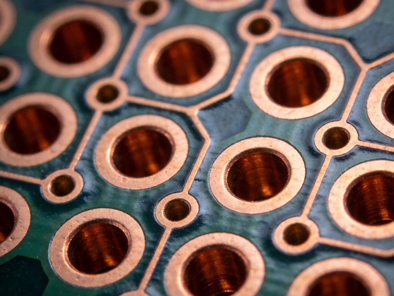
Microvias are one of the defining features of HDI technology and also one of the most common sources of manufacturing problems. Microvias are typically laser-drilled holes that connect adjacent layers, with diameters ranging from 50µm to 150µm. Their small size and the precision required to drill, plate, and fill them make Microvia Design particularly sensitive to DFM violations.
The most common Microvia Design error is specifying an aspect ratio that exceeds manufacturing capabilities. The aspect ratio is the ratio of the via depth (board thickness) to the via diameter. For laser-drilled microvias, the practical aspect ratio limit is typically around 0.8:1 to 1:1, meaning a 100µm diameter via can only be drilled to a depth of about 100µm. Designers who specify deeper microvias than this risk incomplete drilling, Plating Voids, or reliability failures.
To avoid this pitfall, always verify the maximum achievable aspect ratio with your HDI manufacturer before finalizing your design. If you need to connect to deeper layers, use Stacked Microvias (microvias directly on top of each other) or skip vias (microvias that skip one or more layers) instead of trying to create a single deep Microvia.
Microvia lands (pads) must be sized correctly to ensure reliable manufacturing and solder joint formation. Too small a land, and the microvia may not have enough copper for reliable plating or for component attachment. Too large a land, and you lose the density benefits that HDI is designed to provide. Typically, microvia lands should be 200-300µm in diameter for a 100µm microvia, but this varies by manufacturer and technology.
Also ensure that microvias are placed with sufficient clearance from other features. Microvia-to-microvia clearance, microvia-to-trace clearance, and microvia-to-edge clearance all have minimum requirements that must be respected. Crowding microvias too close together can cause manufacturing defects, as the Laser Drilling and subsequent plating processes may not be able to reliably create adjacent structures.
There are several types of microvias in HDI technology—through microvias, blind microvias, buried microvias, and stacked or staggered microvias—and choosing the wrong type for your application can create significant manufacturing challenges. For example, Stacked Microvias (where one microvia sits directly on top of another) require precise Sequential Lamination and drilling, adding cost and complexity. Staggered microvias (offset from each other rather than stacked) are easier to manufacture but require more board area.
Work with your manufacturer early in the design process to determine the most appropriate microvia type for your design, balancing density requirements with manufacturability and cost.
Most Hdi Boards with more than 4-6 layers are built using sequential lamination—where the board is built up in multiple stages, with outer layers added after inner layers are fully processed. This process enables the complex layer structures needed for high-density designs, but it also introduces constraints that must be considered during design.
Each lamination cycle introduces some amount of registration variation, where the layers being added may not align perfectly with the layers already in the board. As more lamination cycles are added, the cumulative registration error can become significant, potentially causing misregistration between features on distant layers.
To minimize registration issues, minimize the number of lamination cycles required for your design. Work with your manufacturer to optimize the layer stackup to reduce the number of build-up stages. Also ensure that critical features are placed on layers that are processed together in the same lamination cycle, rather than spanning multiple cycles where registration error accumulates.
Via-in-pad (VIP) and Buried Via structures are common in HDI designs but require careful DFM consideration. VIP structures, where a via is placed directly in a component pad, require plugging and planarization processes to create a flat surface for component attachment. If not designed correctly, VIPs can cause solder joint voids, component tilt, or reliability issues.
Buried Vias— vias that are fully contained within the board and do not connect to the outer surfaces— require special processing and are not available from all manufacturers. If your design requires buried vias, ensure your manufacturer supports this capability and design your layer stackup accordingly.
Sequential lamination requires careful selection of core thicknesses and prepreg materials for each build-up stage. Using incompatible materials or incorrect thickness combinations can cause delamination, warpage, or dimensional instability during the lamination process. Always verify your material selections with your manufacturer, who will have specific recommendations based on their process capabilities and the specific HDI technology being used.
Material selection is critical for HDI boards, and using the wrong material—or the right material in the wrong way—is a common source of manufacturing problems.
Not all PCB substrates are suitable for HDI manufacturing. Standard FR-4 materials, while widely available and inexpensive, may not have the thermal stability, dimensional stability, or laser drill compatibility required for fine-feature HDI. For advanced Hdi Applications, consider high-performance materials like MEHC (mid-loss high-speed), LLHP (low-loss high-performance), or ceramic-filled substrates that are specifically designed for HDI processes.
When selecting materials, also consider the Tg (glass transition temperature) and Td (thermal decomposition temperature) of the substrate, especially for boards that will undergo multiple reflow cycles during assembly or will be used in high-temperature environments. Low-Tg materials may soften or delaminate during processing or use.
Copper weight and foil profile significantly affect HDI manufacturability. Very thin copper foils (9µm or less) are required for the finest trace widths, but they are more difficult to handle and process. Standard 18µm copper may not be suitable for traces below 75µm. Additionally, the profile of the copper foil (smooth vs. rough) affects adhesion, plating, and Signal Integrity—low-profile foil is generally preferred for HDI to ensure reliable plating and fine-line etching.
The prepregs used between layers in HDI boards must have appropriate resin content and flow characteristics for the build-up process. Too much resin flow can cause fillet formation issues in microvias and Via-in-pad structures. Too little flow can result in voids between layers. Work with your manufacturer to select prepregs with appropriate resin content and flow characteristics for your specific layer structure.
While HDI enables higher density, it also introduces Signal Integrity (SI) and power integrity (PI) challenges that must be addressed in the design stage. Ignoring these requirements can result in boards that fail to function correctly, even if they are manufactured without defects.
HDI boards with fine traces and tight spacing are more susceptible to impedance variation due to manufacturing tolerances. Variations in trace width, trace height, dielectric thickness, and material properties all affect impedance, and these variations are more significant at HDI scales. To ensure reliable Impedance Control, specify wider tolerances for impedance targets, work with your manufacturer to define controlled-impedance structures that are compatible with their process, and validate impedance on production boards through testing.
High-density HDI boards with many ICs and high current demands require careful power delivery network (PDN) design. The thin dielectrics and fine traces used in HDI limit the current-carrying capacity of power planes and traces. Ensure that your power distribution design accounts for the voltage drop and current density limits of HDI structures, and use multiple parallel paths, wider traces, or dedicated power planes to distribute current effectively.
Fine trace spacing in HDI increases the risk of coupling and crosstalk between adjacent signals. Use appropriate spacing rules, ground shielding for sensitive signals, and Differential Pair Routing with controlled spacing to minimize crosstalk. Field solver tools should be used to verify coupling at HDI dimensions, where empirical rules of thumb may not be accurate.
HDI boards are often used in applications with challenging thermal and reliability requirements, including automotive, aerospace, and medical environments. Designing without accounting for these requirements can result in boards that pass manufacturing but fail prematurely in the field.
The high density of HDI boards makes Thermal Management more challenging, as there is less space available for heat spreading and dissipation. When placing high-power components on HDI boards, ensure that Thermal Vias, copper planes, and heat sinks are used to effectively move heat away from components. Also consider the thermal resistance of the Hdi Stackup and ensure that the materials selected can tolerate the operating temperatures expected in your application.
HDI boards with many microvias and fine features are more susceptible to fatigue failure under thermal cycling than conventional boards. The thermal coefficient of expansion (TCE) mismatch between copper, substrate, and components can cause stress on microvia barrels and solder joints during thermal cycling, potentially leading to cracking and failure over time.
To improve thermal reliability, select materials with TCE values that closely match the components being used, minimize the number of thermal cycles during assembly, and consider using thermally robust microvia designs (like teardrop pads or reinforced land structures) where stress concentrations are highest.
HDI boards, particularly those using thin cores and build-up layers, can be more sensitive to moisture absorption than conventional boards. Moisture in the board during reflow soldering can vaporize and cause delamination, blistering, or microvia damage. Ensure that HDI boards are properly dried before assembly, and select materials with low moisture absorption characteristics for moisture-sensitive applications.
One of the most preventable HDI DFM pitfalls is designing features that exceed the manufacturing capabilities of your chosen manufacturer. HDI capabilities vary significantly between manufacturers, and designing to the theoretical limits of HDI technology rather than to your manufacturer's specific capabilities is a recipe for respins and manufacturing failures.
Before starting your HDI design, engage with your manufacturer to understand their specific HDI capabilities, including minimum trace width and spacing, minimum microvia diameter and depth, maximum layer count and minimum board thickness, supported materials and finishes, and registration and tolerance capabilities. Do not assume that published capability specifications represent what is reliably achievable on production boards— build in a safety margin and verify with your manufacturer.
HDI manufacturers are typically tiered by capability—entry-level HDI manufacturers may support 4-6 layer boards with 100µm traces and 150µm microvias, while advanced manufacturers can produce 20+ layer boards with 50µm traces and 75µm microvias. Match your design complexity to a manufacturer with appropriate capability tier, rather than trying to force an advanced design through a manufacturer who cannot reliably produce it.
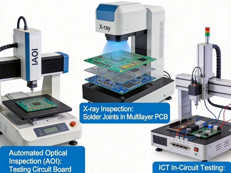
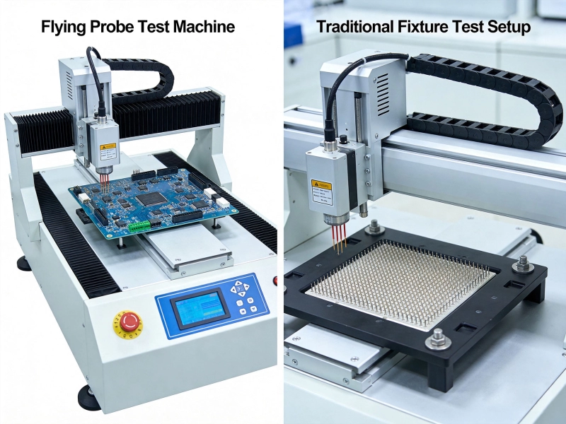
HDI boards are more difficult to test than conventional boards due to their high density and limited access to internal nodes. Incorporate testability into your design from the beginning, including test points for critical signals, probe-accessible structures for in-circuit testing, and design for flying probe or Boundary Scan testing where physical access is limited. Failing to plan for testing can result in boards that cannot be adequately verified before shipment.
Even the best-designed HDI board can fail if there is poor communication with the manufacturer. Ambiguous design files, missing information, and assumptions about manufacturing capabilities are common sources of manufacturing problems.
Ensure that your design data package includes all necessary files: complete Gerber files for all layers, drill files in Excellon format, netlist and BOM with complete part numbers and quantities, stackup diagram and impedance specifications, material specifications and preferred manufacturer list, assembly drawings with special instructions, and any critical requirements or tolerances not captured in the design files. Ambiguous or incomplete data leads to assumptions, and assumptions lead to errors.
Always request a DFM review from your HDI manufacturer before finalizing your design for production. Most reputable HDI manufacturers offer free DFM analysis that identifies potential manufacturing issues, suggests design optimizations, and confirms that the design is within their manufacturing capabilities. Review this feedback carefully and address all issues before proceeding to production.
Even with perfect DFM practices, always validate your HDI design with prototypes before committing to mass production. Prototypes allow you to verify that the board functions correctly, that assembly processes work as expected, and that there are no unexpected manufacturing issues. Use prototype results to refine your design and manufacturing process before scaling up to production volumes.
Based on the common pitfalls outlined above, here is a summary of best practices for successful HDI design:
Hdi Pcb design presents unique challenges that require a thorough understanding of both the technology and the manufacturing process to navigate successfully. By understanding the common pitfalls outlined in this article—microvia design errors, sequential lamination issues, material selection mistakes, signal integrity oversights, Thermal Management failures, and communication breakdowns—you can design HDI boards that are not only functionally superior but also reliably manufacturable.
The key to HDI DFM success is partnership with your manufacturer. The most successful HDI designs emerge from close collaboration between the design team and manufacturing engineers, where manufacturing expertise informs design decisions from the earliest stages. By building this partnership and following HDI-specific DFM best practices, you can avoid the costly pitfalls that derail so many HDI projects and bring your advanced electronic products to market faster, at lower cost, and with greater reliability.
A: The minimum reliably manufacturable microvia size depends on the manufacturer's capabilities and the specific HDI technology being used. Most manufacturers can reliably produce 100µm microvias, with advanced manufacturers achieving 75µm or smaller. Always verify with your specific manufacturer and design with a safety margin above their minimum capability.
A: There is no fixed limit, but each additional lamination cycle adds cost, lead time, and cumulative registration error. For practical purposes, most manufacturers recommend limiting HDI designs to 4-6 build-up stages (lamination cycles) to balance density requirements with manufacturability and cost. More complex structures may require specialized processes or alternative approaches like embedded active components.
A: Most standard surface finishes are compatible with HDI, including ENIG (electroless nickel immersion gold), Immersion Silver, Immersion Tin, and OSP (organic solderability preservative). However, the choice of surface finish may be constrained by your specific HDI process—for example, some microvia structures may require specific finishes for reliability. Discuss surface finish options with your manufacturer early in the design process.
A: Field reliability depends on proper design practices for your specific application environment. Work with your manufacturer to conduct appropriate reliability testing for your application's requirements, including thermal cycling, thermal shock, humidity exposure, vibration testing, and mechanical stress testing. Materials selection, stackup design, and thermal management all contribute to long-term reliability and should be considered from the design stage.
The Art of Microvia Placement: Staggered vs. Stacked ViasSeptember/24/2026
Mastering Stack-up Design for Optimal HDI PerformanceJune/08/2026
Designing HDI Backplanes for High-Performance Networking EquipmentOctober/16/2026
Advanced Testing Methods for High-Density Interconnect PCBsMay/28/2026
Best Practices for BGA Fanout and Routing in HDI LayoutsJuly/07/2026
Flying Probe vs. Fixture Testing: Which is Best for HDI PCBs?June/11/2026
Overcoming the Challenges of Testing Fine-Pitch BGA on HDISeptember/04/2026
The Importance of Electrical Testing for Microvia ReliabilityJuly/09/2026