Open Nav

As electronics devices continue their relentless march toward Miniaturization, the printed circuit boards inside them face increasing pressure to deliver more functionality in smaller footprints. High Density Interconnect (HDI) printed circuit boards, powered by Microvia Technology, have emerged as the enabling technology behind smartphones, wearables, medical implants, and countless other compact electronic products. Understanding Microvia Technology becomes essential for any engineer working on next-generation electronic designs. This introduction covers the fundamentals: what Microvias are, how they differ from traditional vias, manufacturing approaches, design considerations, and the applications driving their adoption.
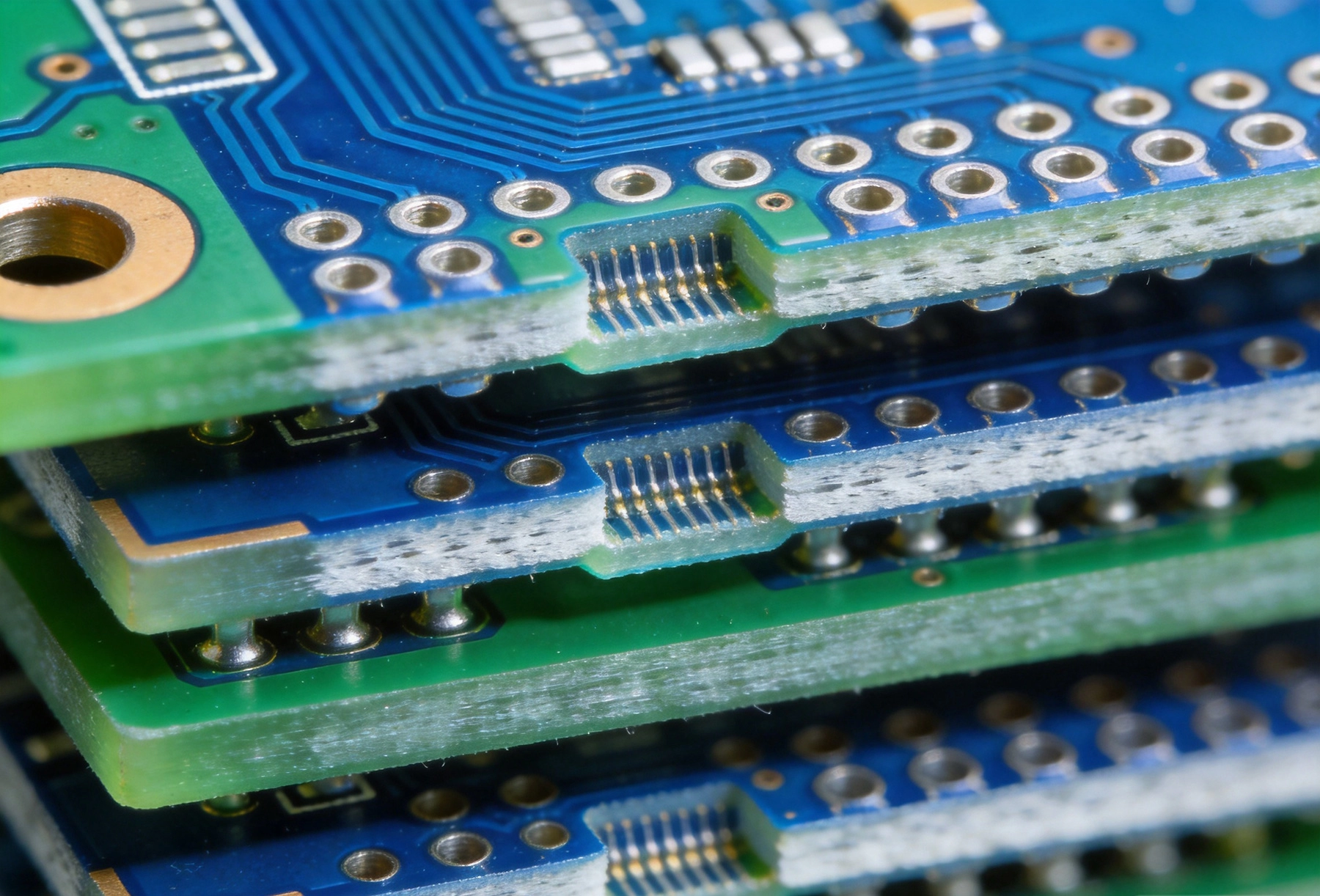
Microvias represent a specific category of via structures distinguished primarily by their dimensions. The IPC (Institute for Printed Circuits) standards define microvias as vias with diameters typically below 0.15mm (150 microns), though industry practice often extends this threshold to 0.20mm or even 0.25mm depending on the manufacturing capability and specific application requirements.
The defining characteristic of a Microvia is its aspect ratio—the ratio of depth to diameter. Microvias maintain low aspect ratios, generally 1:1 or less, meaning their depth does not exceed their diameter. This constraint exists because microvias are created using laser ablation rather than mechanical drilling, and the laser cannot reliably remove material at depths significantly exceeding the spot size throughout the hole diameter.
Traditional plated through-hole (PTH) vias connect traces on outer layers to inner layers throughout the entire board thickness. These vias are mechanically drilled after the board is laminated and require significant drilling time, generate substantial drill wear, and consume notable board real estate due to their land (pad) requirements.
Microvias differ fundamentally in several ways:
Hdi Pcb designs employ several distinct Microvia configurations, each suited to particular routing strategies and manufacturing approaches.
Stacked microvias directly overlie one another, connecting sequential layer pairs. A typical stack might connect layers 1-2, then 2-3, then 3-4 in a vertical column. This arrangement maximizes routing density in a specific location but requires careful attention to barrel plating and fill materials to ensure reliability during thermal cycling.
Stacked microvia structures are common in chip-on-board designs, package-on-package (PoP) assemblies, and areas where maximum component density is required, such as beneath BGA packages.
Staggered microvias offset between layer pairs rather than stacking directly on top of each other. For example, a microvia connecting layers 1-2 might be offset from another connecting layers 3-4, with the connection between 2-3 made through a Buried Via or trace routing.
This configuration offers improved reliability compared to fully stacked arrangements because thermal stress is distributed across a larger area. Staggered microvias remain popular in consumer electronics where moderate density increases are needed without the full complexity of fully stacked designs.
Skip vias (sometimes called skip-layer vias) bypass intermediate layers while maintaining microvia dimensions. For instance, a laser-drilled via might connect layer 1 directly to layer 4, skipping layers 2 and 3. This requires careful process control to ensure reliable plating through the longer depth while maintaining the diameter constraints of microvia technology.
HDI board construction leverages microvia technology to create layer counts that would be impractical or impossible with traditional through-hole via technology alone.
Build-up construction: The most common HDI approach builds layers sequentially on a core substrate. The core provides mechanical stability while build-up layers can employ microvia technology. Typical constructions include "1+N+1" (one build-up layer on each side of the core) and "2+N+2" (two build-up layers per side).
Coreless construction: Advanced HDI designs eliminate the traditional core entirely, building all layers using Sequential Lamination and microvia formation. This approach enables the highest density but requires sophisticated manufacturing capabilities and careful attention to warpage control.
Hybrid constructions: Many practical designs combine traditional through-hole via technology for power and ground distribution with microvia technology for high-speed signal routing. This hybrid approach balances manufacturing cost with electrical performance requirements.
The IPC defines specific HDI stack-up classifications that provide common terminology for describing microvia implementations:
Any-layer HDI (sometimes called "any-layer stacked") represents the highest density implementation, where microvia stacks provide connections between any two layers in the board, not just adjacent pairs.
The creation of microvias depends on laser ablation technology that vaporizes Dielectric Material rather than mechanically removing it as with traditional drill bits.
Two primary laser types dominate microvia formation:
CO2 lasers operate at 10.6μm wavelength and are well-absorbed by organic dielectric materials. They excel at removing base resin but may leave carbonized residue requiring cleaning steps. CO2 lasers are cost-effective for standard HDI production.
UV lasers operate at 355nm wavelength and photo-ablate material through a photochemical rather than purely thermal process. This produces cleaner hole walls with minimal residue and is essential for advanced microvia applications, particularly in filled-via processes. UV laser systems carry higher capital and operating costs.
Creating Hdi Boards with microvias requires multiple sequential steps:
Each cycle adds cost and cycle time but enables density increases that would be impossible in traditional board construction.
Advanced Hdi Applications often require filled microvias where the via barrel is completely filled with conductive or non-conductive material and the surface is planarized (ground flat) to provide a flat landing surface for component mounting.
Conductive fill materials (typically copper-filled) enable microvias to function as Thermal Vias or to carry higher current. Non-conductive fills (epoxy or polymer) provide mechanical stability and enable subsequent layer formation over the filled structure.
Successful HDI design with microvias requires attention to manufacturing constraints and electrical requirements that differ from Traditional Pcb design.
Design rules for microvia-based boards differ from standard multilayer constraints:
Microvia technology affects thermal performance in complex ways. While microvias reduce thermal mass and can improve heat spreading through shorter thermal paths, they also reduce copper cross-section for current carrying compared to larger through-hole vias.
Designers must carefully calculate current requirements and ensure adequate copper plating thickness in microvia barrels to prevent electromigration failures, particularly in high-current applications.
Microvia technology offers significant Signal Integrity advantages for high-speed designs:
These advantages come with tradeoffs: the smaller structures are more sensitive to manufacturing variations, and Impedance Control requires tighter process control than traditional through-hole boards.
Microvia Reliability has historically been a concern, but manufacturing process improvements have established microvia technology as highly reliable for most applications when properly designed and manufactured.
Microvia barrels experience different stress distributions than through-hole vias during thermal cycling. The stress concentrates at the interface between the microvia barrel and the landing pad, and designs with adequate annular ring and barrel diameter ratios demonstrate excellent thermal cycling performance.
Industry experience has established that properly designed stacked microvia structures can exceed 1,000 thermal cycles (-40°C to +125°C) without failure in typical consumer electronics applications. More demanding thermal environments may require additional design accommodations or alternative configurations.
Common microvia failure modes include:
Several application categories have driven aggressive adoption of microvia technology and continue to push the boundaries of HDI capability.
The smartphone industry represents the largest volume application for HDI microvia technology. Die-stacked packages, high-pin-count application processors, and RF modules all depend on microvia density to achieve their form factors. The continuous pressure to add features while reducing device thickness ensures ongoing investment in advanced HDI capabilities.
Smartwatches, fitness trackers, and other wearable devices push Hdi Technology toward even smaller form factors with demanding requirements for flex or rigid-flex constructions. Microvia technology enables the high-density routing necessary to connect multiple sensors, processors, and displays within severely constrained physical envelopes.
Implantable medical devices such as pacemakers, cochlear implants, and neurostimulators require extremely small form factors with high reliability. Hdi Technology enables the Miniaturization that makes these devices practical while meeting the stringent reliability requirements of medical applications.
The semiconductor industry's transition to advanced packaging (including 2.5D interposers and embedded die structures) creates opportunities for HDI substrates that serve as intermediaries between chip-level and board-level interconnect. These applications demand the finest microvia capabilities that current manufacturing can achieve.
Microvia technology has transformed printed circuit board design from a relatively static discipline into a dynamic field where board architecture directly impacts product capability and differentiation. Understanding the fundamentals—microvia types, HDI construction approaches, manufacturing processes, and design constraints—provides the foundation for leveraging this technology effectively.
As electronic products continue demanding greater functionality in smaller packages, microvia technology will remain central to achieving these goals. Engineers who master HDI design principles position themselves to create products that would be impossible using Traditional Pcb approaches alone. The investment in understanding microvia technology pays dividends across an increasingly wide range of electronic applications.
Leading-edge HDI manufacturers can produce microvias as small as 50-60μm in diameter, though these represent the extreme edge of current capability. Standard production typically operates in the 100-150μm range. The minimum size is constrained by laser spot size, material properties, and the aspect ratio limits of reliable plating processes.
Microvia technology adds significant cost compared to traditional through-hole multilayer boards. Each build-up layer adds process steps, and laser ablation equipment carries higher capital and operating costs than mechanical drilling. However, the density advantages often enable overall cost reduction by shrinking board size and reducing layer count compared to equivalent traditional designs.
Microvia current-carrying capacity depends on barrel plating thickness and via diameter. While individual microvias cannot match the current capacity of larger through-hole vias, Thermal Vias using conductive fill materials can effectively spread heat. Design calculations should account for current density limits and incorporate sufficient microvia counts for high-current applications.
Standard HDI typically connects only adjacent layers using microvia technology, with some layer connections made through traditional buried vias in the core. Any-layer HDI uses microvia stacks to connect any layer to any other layer throughout the board, eliminating the need for buried vias and enabling the highest routing density. Any-layer construction requires more sophisticated manufacturing but provides maximum design flexibility.
Designs that benefit from HDI technology typically exhibit one or more of the following characteristics: BGA packages with pitch below 0.5mm, need for more than 4 layers in a thickness below 1.2mm, high-frequency signals requiring controlled impedance with minimal via stub effects, and space or weight constraints that require maximizing routing density per unit area.
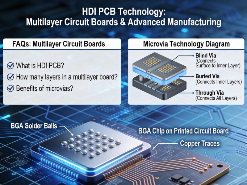
Top 10 Frequently Asked Questions About HDI PCB TechnologyMay/28/2026
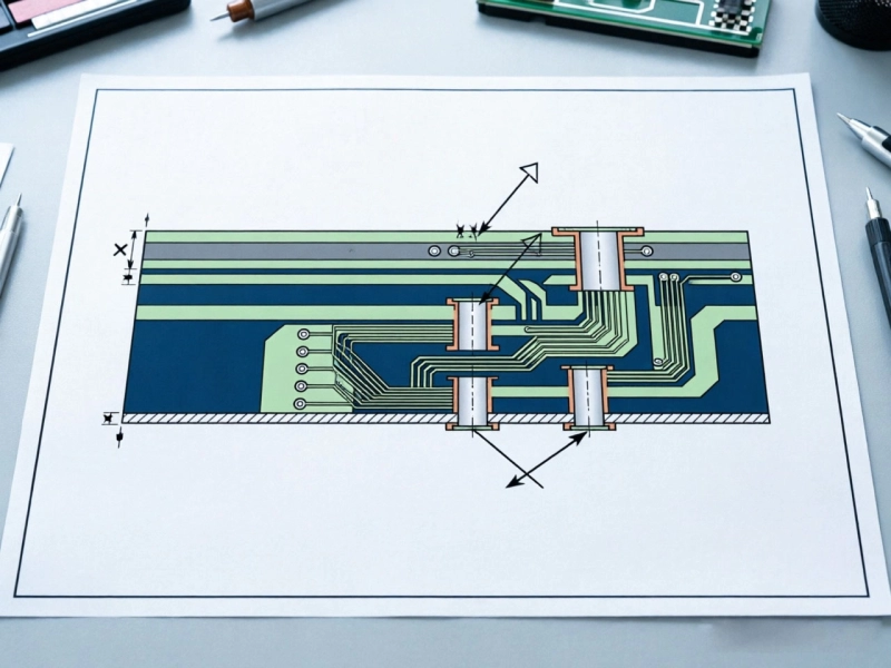
How to Read and Interpret HDI PCB Stack-up Drawings?July/14/2026
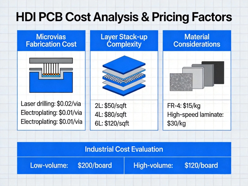
HDI PCB Cost Guide: What Factors Drive the Price Up?June/16/2026

Implementing a Robust Quality Control System for HDI ManufacturingJune/15/2026
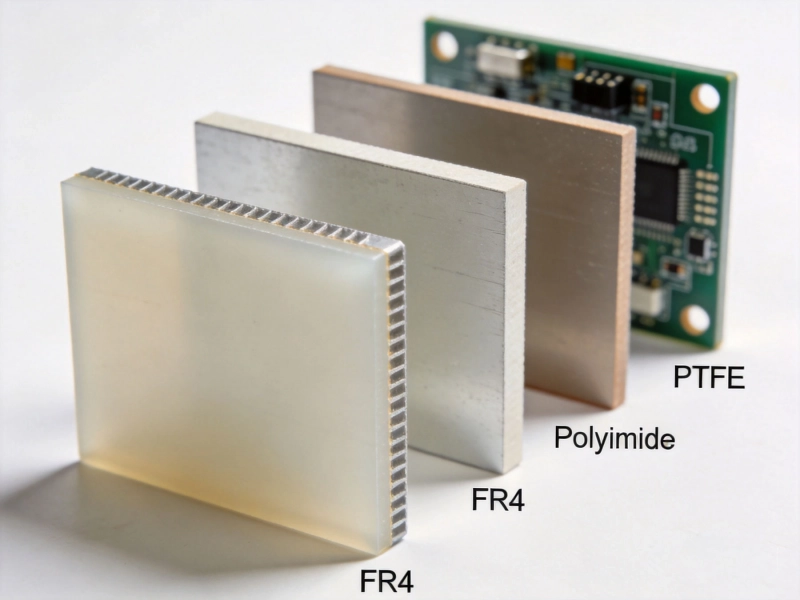
Selecting the Right Dielectric Materials for High-Performance HDI PCBsMay/28/2026
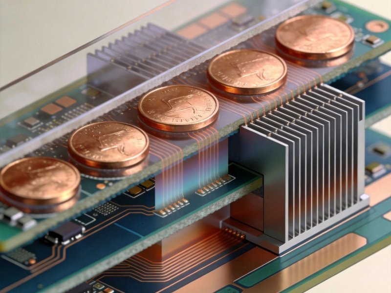
Copper Coin and Embedded Heat Sinks: Advanced Cooling for HDIJuly/08/2026
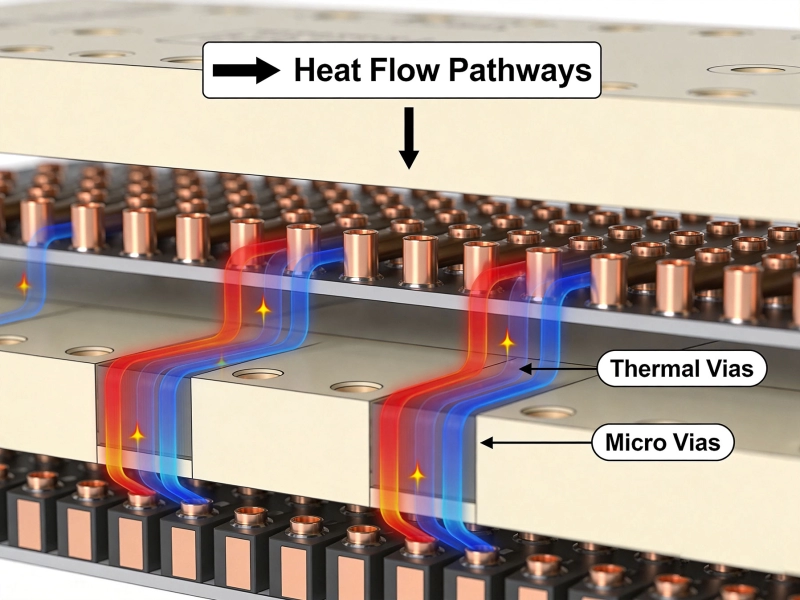
The Role of Thermal Vias in Dissipating Heat from HDI BoardsJune/09/2026
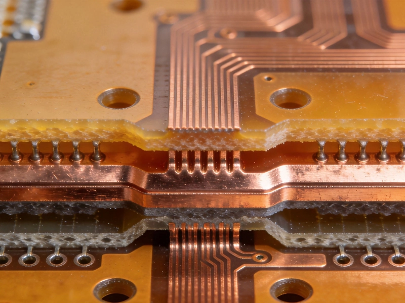
FR-4 vs. High-Tg Materials: What Works Best for HDI Applications?July/07/2026