Open Nav

High Density Interconnect (HDI) boards have revolutionized modern electronics by enabling unprecedented Miniaturization and performance in smartphones, tablets, and advanced computing systems. However, the same dense packing of components and routing that makes Hdi Technology powerful also creates significant Thermal Management challenges. Heat generated by active components must find efficient pathways to escape the board, or reliability suffers dramatically.
Thermal Vias serve as critical heat transfer channels in Hdi Boards, conducting thermal energy from heat-generating components to external heat sinks, ground planes, or the board surface where convective cooling can remove it. Understanding how to properly implement Thermal Vias determines whether an HDI design achieves its performance goals or fails prematurely due to overheating.
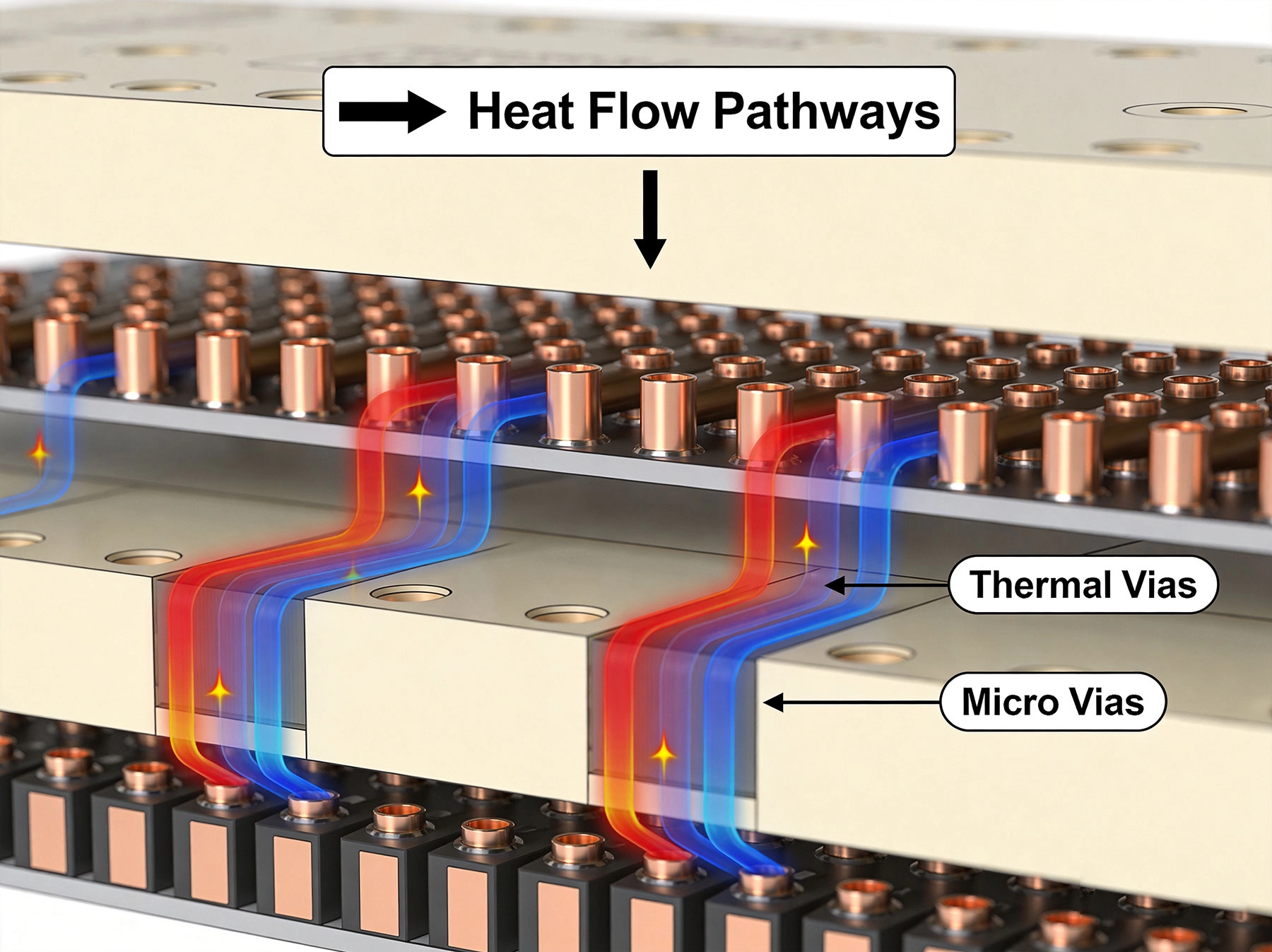
Thermal vias are plated-through holes strategically placed beneath components to enhance vertical heat flow. Unlike standard through-hole vias that primarily serve electrical connections, thermal vias are optimized for thermal conductivity. The Copper Plating lining the via barrel creates an excellent thermal pathway, typically providing thermal conductivity of 380-400 W/mK compared to the 0.3-0.5 W/mK of standard PCB substrate materials.
The construction of thermal vias differs from standard vias in several important ways. Thermal vias typically use larger diameters to maximize Copper Plating surface area and minimize thermal resistance. While standard Microvias in Hdi Boards may measure 100-150μm in diameter, thermal vias often range from 200μm to 500μm or larger, depending on available space and thermal requirements.
The copper plating thickness in thermal vias is often increased beyond standard plating specifications to further reduce thermal resistance. Standard IPC Class 2 plating specifies minimum 25μm copper, but thermal vias may receive 30-40μm or even heavier plating to maximize heat transfer capacity. This additional copper not only improves Thermal Performance but also enhances mechanical reliability.
HDI boards present unique opportunities and challenges for thermal via implementation. The Sequential Lamination process used to create HDI stackups allows thermal vias to connect specific layers rather than spanning the entire board thickness. This selective connection reduces thermal resistance by eliminating unnecessary substrate segments from the heat path.
Skip-via construction, where vias connect non-adjacent layers, is commonly employed in Thermal Management applications. A thermal via might connect layer 1 directly to layer 8, bypassing intermediate signal layers and minimizing the thermal resistance path. This approach proves particularly valuable when the heat source sits on an outer layer but thermal dissipation must reach an internal ground plane or opposite surface.
The fundamental advantage of Hdi Technology—increased routing density—also creates thermal density challenges. Components that might spread across multiple boards in conventional designs are packed into compact spaces on HDI boards. This concentration means multiple heat sources may overlap thermally, creating hotspots that exceed individual component thermal budgets.
The thermal resistance from junction to case (Rjc) specifications for modern components continue decreasing as packages shrink, meaning components generate more heat per unit area. Without effective thermal management, these concentrated heat sources can exceed maximum junction temperatures, leading to accelerated failure mechanisms including electromigration, dielectric breakdown, and solder joint fatigue.
While HDI boards enable smaller end products, the reduced board area limits available surface for convective cooling. A Smartphone Pcb measuring 100mm × 60mm cannot dissipate heat the same way a 300mm × 200mm board might. Thermal vias provide the only practical means for transferring heat away from components on space-constrained HDI boards.
The situation becomes more challenging when thermal vias must compete with signal routing for limited routing channels. Strategic thermal via placement requires early planning in the design phase, as retrofitting thermal management after board layout completion often proves difficult or impossible without significant redesign.
Components placed near heat-generating devices experience elevated ambient temperatures that affect their reliability and performance. The thermal coupling between adjacent components depends on board material properties, component placement density, and the effectiveness of thermal vias in spreading the heat laterally before it reaches sensitive devices.
Thermal Simulation during design helps identify potential coupling issues before hardware is built. CFD (Computational Fluid Dynamics) analysis of board temperatures reveals whether thermal vias provide adequate spreading or whether additional mitigation measures such as thermal isolation, shielding, or alternative component placement might be necessary.
Single thermal vias rarely provide sufficient heat dissipation for power components. Thermal via arrays, sometimes called thermal thrupaks or thermal pads, spread heat transfer across multiple parallel pathways. Common configurations include square or circular arrays beneath QFN and PowerPAD packages, and perimeter arrays around large BGA thermal pads.
The number of thermal vias required depends on the thermal power dissipation, acceptable temperature rise, and available area. A rule of thumb suggests 16-36 thermal vias for typical power packages, but high-power applications may require 100 or more thermal vias arranged in optimized patterns. Always reference manufacturer thermal recommendations when available.
Via spacing affects both thermal spreading and manufacturing considerations. Tighter via spacing improves thermal spreading but may compromise board manufacturing yield. IPC guidelines specify minimum spacing requirements based on board thickness and manufacturing capability, but thermal via arrays often push these limits.
Staggered via patterns typically provide better thermal spreading than aligned patterns because they distribute copper more uniformly across the thermal pad area. The trade-off involves slightly reduced thermal cross-section per unit area compared to packed circular patterns, but improved manufacturing yield often justifies this compromise.
Thermal vias connected to exposed thermal pads must be properly treated to prevent solder wicking during assembly. Solder flowing down via barrels creates voids in the solder joint that compromise both electrical and thermal connections. Several approaches address this issue depending on the thermal pad configuration.
Capillary Action Suppression (CAS) Via Filling with conductive or non-conductive epoxy prevents solder wicking while maintaining thermal conductivity through the copper plating. Via-in-pad with plugged or plated-over construction creates a smooth surface suitable for direct component mounting. Alternatively, dog-bone routing separates vias from the direct thermal pad area while maintaining thermal connection through the underlying copper plane.
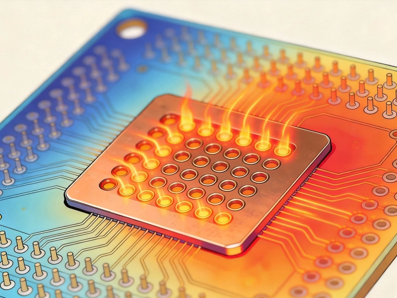
Via-in-pad technology places thermal vias directly beneath component thermal pads, eliminating the thermal resistance of surface copper traces. This approach provides the shortest possible thermal path from component to internal heat-spreading planes. However, via-in-pad requires special processing to prevent solder wicking and ensure reliable solder joints.
Via Filling processes include screen printing conductive paste into vias, vacuum filling with non-conductive epoxy, and plating-over closed vias. Each approach offers different cost-performance trade-offs. Conductive fill provides the best Thermal Performance but at higher cost, while plated-over construction offers a cost-effective compromise for many applications.
Thermal via stitching connects multiple internal planes to create robust thermal pathways. For multi-layer boards with separate ground and power planes, stitching thermal vias through the entire stackup creates redundant thermal paths that continue functioning even if individual planes are interrupted by routing channels.
Stitching also connects thermal planes on opposite sides of the board, enabling heat transfer from components mounted on one side to a heat sink attached to the opposite side. This technique proves particularly valuable for double-sided assembly where thermal components are placed on both board surfaces.
HDI technology enables blind thermal vias that connect outer layers to specific internal layers without penetrating the full board thickness. This capability reduces thermal resistance by eliminating unnecessary thermal resistance from layers that do not contribute to heat spreading. For example, a Blind Via connecting layer 1 to layer 4 eliminates thermal resistance through layers 5 through the complete board thickness.
Buried thermal vias connect internal layers without any external connection, useful for creating internal thermal planes that distribute heat from mid-layer components to outer-layer thermal vias for final dissipation. The combination of blind and buried thermal vias creates sophisticated thermal management architectures in complex HDI designs.
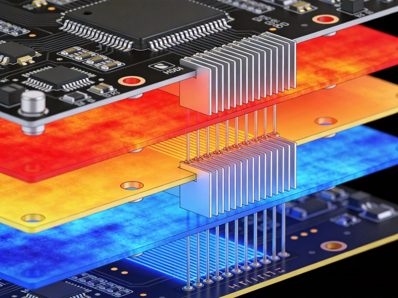
Thermal Simulation has become essential for complex HDI designs where trial-and-error thermal optimization is impractical. CFD tools can model heat transfer from components through thermal vias to external boundaries, predicting temperature distributions throughout the board under various operating conditions.
Accurate thermal simulation requires detailed component power dissipation data, board material properties (including temperature-dependent thermal conductivity), boundary conditions representing actual operating environments, and accurate representation of thermal via configurations. GIGO (Garbage In, Garbage Out) applies strongly to thermal simulation—poor input data produces poor predictions regardless of tool sophistication.
Some high-power applications require thermal enhancement beyond what standard Pcb Technology can provide. Metal-core PCBs (MCPCBs) with aluminum or copper substrates provide thermal conductivity values of 1-5 W/mK, significantly better than standard laminates. However, metal-core boards sacrifice the routing density that makes HDI technology valuable.
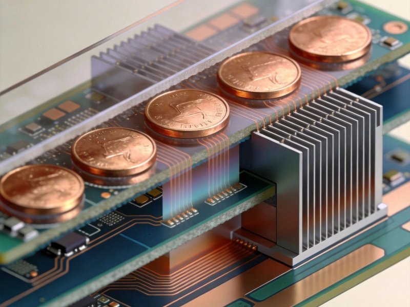
Alternative approaches include thick copper layers (2-4 oz) for improved lateral spreading, ceramic-filled substrates with higher thermal conductivity, and embedded metal coins that provide direct thermal pathways. Each approach involves trade-offs between thermal performance, cost, and manufacturing complexity that must be evaluated for specific applications.
Physical thermal testing validates simulation predictions and identifies issues not captured in analytical models. Thermal test points placed strategically on production boards enable temperature monitoring during operation, verifying that designs meet thermal targets under real-world conditions.
Infrared thermography provides non-contact thermal mapping of operating boards, revealing hotspots and temperature distributions that might be missed by point measurements. Liquid crystal thermal imaging offers higher resolution for small-scale thermal patterns but requires controlled heating sequences. Both techniques help validate thermal via effectiveness and identify opportunities for optimization.
Thermal via reliability depends critically on plating quality. Void-free copper plating throughout the via barrel ensures consistent thermal conductivity without hot spots that might cause premature failure. X-ray Inspection verifies plating uniformity before assembly, while cross-section analysis of sample vias confirms plating integrity.
Thermal cycling exposes thermal via weaknesses through coefficient of thermal expansion (CTE) mismatches between copper plating and substrate material. High-quality plating with proper adhesion survives thermal cycling without barrel cracking, but marginal plating may pass initial testing only to fail during field use. Accelerated thermal cycling testing of samples validates thermal via reliability for demanding applications.
Thermal via dimensions must satisfy manufacturing aspect ratio limitations. The ratio of via depth to diameter determines whether reliable plating can be achieved. Standard PCB processes typically limit aspect ratios to 10:1 or 12:1, meaning a 300μm diameter via can be drilled to maximum 3.0-3.6mm depth. HDI processes with Sequential Lamination may relax these limitations for Blind Vias.
When thermal requirements exceed manufacturing capabilities, multiple shorter thermal vias can be stacked or staggered to achieve effective thermal paths that would be impossible with single vias. This approach increases design complexity but may be necessary for extreme thermal management requirements.
Thermal via implementation affects manufacturing cost in multiple ways. Additional drilling operations, heavier copper plating, via filling processes, and potential plating-over requirements all add to board cost. Densely populated thermal via arrays significantly impact manufacturing time and yield, translating directly to higher unit costs.
Early cost estimation helps balance thermal performance against budget constraints. Sometimes a smaller number of larger thermal vias provides adequate thermal management at lower cost than many small vias. Strategic placement focusing thermal vias in the most effective locations may achieve target thermal performance with fewer vias than blanket coverage approaches.
Phase change materials (PCMs) embedded within thermal via structures provide thermal capacitance that absorbs transient heat spikes before temperatures rise to damaging levels. PCM thermal vias store thermal energy during high-power events, releasing it during cool-down periods when convective cooling can remove the heat.
PCM integration typically involves filling thermal vias with paraffin-based or fatty acid-based materials that melt at specific temperatures. The latent heat of fusion provides high thermal storage capacity within a narrow temperature range. This approach proves particularly valuable for applications with intermittent high-power operation.
Vapor chamber technology, well-established in heat sink applications, has been adapted for PCB embedding. Vapor chambers consist of sealed cavities containing small quantities of working fluid that evaporate and condense to transport heat with very low thermal resistance. Embedding vapor chambers within HDI boards enables unprecedented thermal spreading from concentrated heat sources.
While vapor chamber PCBs involve significant manufacturing complexity and cost, they provide thermal performance approaching two-phase cooling with a form factor compatible with standard PCB assembly processes. This technology remains niche but offers thermal management options for extreme applications where conventional approaches prove inadequate.
Passive thermal management through thermal vias and heat sinks reaches practical limits in some applications. Active cooling integration, including embedded thermoelectric coolers (TECs) or micro-fluidic channels, provides thermal management capability beyond passive approaches. These technologies enable precise temperature control alongside heat removal.
Thermal vias can transport heat to or from active cooling elements positioned on the board surface or embedded within the stackup. This hybrid approach combines passive spreading through thermal vias with active temperature regulation for applications requiring tight thermal control such as laser diode drivers, RF power amplifiers, or optical sensor assemblies.
Power Electronics applications involving MOSFETs, IGBTs, and voltage regulators require aggressive thermal management due to high power dissipation levels. Thermal vias beneath power packages must handle current levels that create significant self-heating within the thermal via itself. Thermal via current density limits may constrain the number of parallel paths required for adequate heat dissipation.
Wide copper pours connected to thermal via arrays provide lateral heat spreading that reduces thermal via current density requirements. Some designs incorporate copper coin embedding where the thermal pad sits directly on thick copper rather than standard laminate, providing immediate thermal spreading before heat must traverse thermal vias.
RF and microwave applications present unique thermal challenges because thermal vias can affect electrical performance. Thermal via proximity to transmission lines may introduce parasitic capacitance or inductance that detunes critical circuits. Careful thermal via placement considering electromagnetic effects ensures thermal management does not compromise RF performance.
Thermal vias in ground planes near sensitive circuits should be stitched to multiple ground references to prevent them from acting as slot antennas or creating unintended coupling paths. The trade-off between thermal performance and electrical parasitics requires careful simulation and optimization for RF applications.
High-brightness LEDs generate significant heat that directly affects luminous output, color stability, and operational lifetime. LED junction temperature specifications typically require maintaining temperatures below 85-100°C for acceptable performance. Thermal via implementation beneath LED mounting pads provides the primary thermal pathway for most LED assemblies.
Metal-core PCBs or metal-backed flexible circuits commonly support high-power LED arrays, with thermal vias connecting the LED mounting surface to the metal backing for effective heat spreading. The thermal path from LED junction through thermal vias, substrate, and metal backing to ambient must be designed holistically to achieve target junction temperatures.
Thermal vias play an indispensable role in dissipating heat from HDI boards, enabling the continued Miniaturization of electronic products while maintaining acceptable operating temperatures. The effectiveness of thermal via implementations depends on proper design from the earliest stages of product development, appropriate manufacturing processes, and thorough validation of thermal performance.
As component power densities continue increasing and HDI boards become even more compact, thermal management becomes increasingly critical to product success. Understanding thermal via design guidelines, manufacturing capabilities, and advanced thermal management strategies positions engineering teams to create reliable products that meet market demands for performance and miniaturization.
The investment in proper thermal via design pays dividends through improved reliability, extended product lifetime, and reduced field failures. By treating thermal management as a first-class design constraint rather than an afterthought, engineers can achieve thermal performance targets while maintaining the routing density that makes HDI technology valuable.
Thermal via thermal resistance varies widely based on dimensions, plating thickness, and board construction. A typical 300μm diameter thermal via with standard plating might exhibit 20-40°C/W thermal resistance. Larger vias with heavy plating can achieve 5-15°C/W, while filled thermal vias may drop below 5°C/W. Arrays of parallel thermal vias reduce effective thermal resistance proportionally.
QFN thermal pad thermal via requirements depend on power dissipation and acceptable temperature rise. Typical recommendations range from 16 to 36 thermal vias for standard packages, with larger packages or higher power requiring more thermal vias. Always consult package manufacturer thermal guidelines when available.
Thermal vias can affect high-speed Signal Integrity if placed improperly near sensitive transmission lines. Thermal via anti-pads should be carefully managed to prevent capacitance effects, and thermal via placement near differential pairs requires attention to coupling effects. For most power and low-speed signals, thermal via placement does not significantly impact signal quality.
Thermal vias are optimized for heat transfer rather than electrical connection. They typically use larger diameters and heavier copper plating than standard vias. Thermal vias often appear in arrays beneath thermal pads rather than for signal routing, and they may be filled or plated-over to prevent solder wicking.
Several techniques prevent solder wicking: conductive or non-conductive via filling with epoxy, plated-over closed vias, tenting with solder mask, or dog-bone routing that separates vias from direct thermal pad contact. The chosen method depends on thermal requirements, manufacturing capability, and cost constraints.
Copper Coin and Embedded Heat Sinks: Advanced Cooling for HDIJuly/08/2026
The Impact of Via-in-Pad on Thermal Performance and ReliabilitySeptember/26/2026
Effective Thermal Management Strategies for High-Density PCBsMay/28/2026
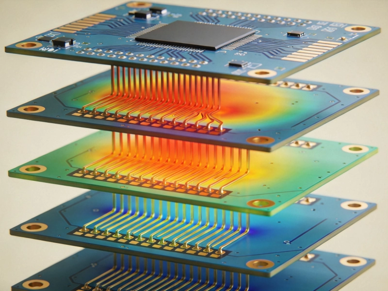
How to Use Thermal Simulation Software to Optimize HDI LayoutsJuly/29/2026
Managing Heat in High-Power HDI Applications: A Practical GuideSeptember/03/2026
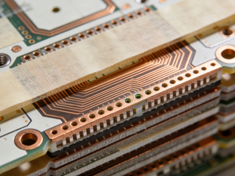
Exploring the 6 Types of HDI Structures: From Type I to Any-LayerAugust/14/2026
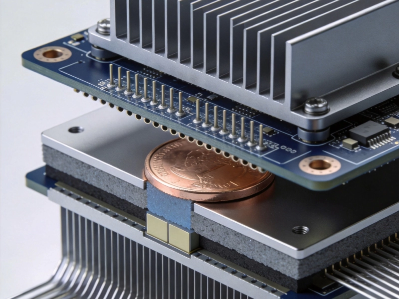
Thermal Management Strategies for HDI Power ModulesSeptember/11/2026
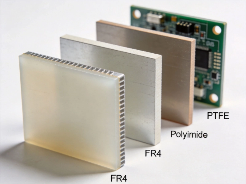
Selecting the Right Dielectric Materials for High-Performance HDI PCBsMay/28/2026