Open Nav

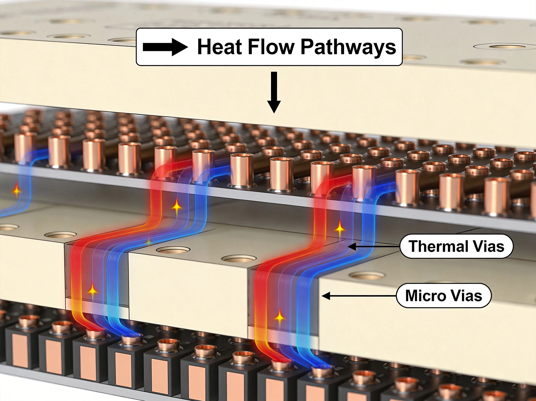
High Density Interconnect (HDI) boards have revolutionized modern electronics by enabling unprecedented miniaturization and performance in smartphones, tablets, and advanced computing systems. However, the same dense packing of components and rou...
https://www.high-density-interconnect-pcb.comhttps://www.high-density-interconnect-pcb.com/hdi-pcb-thermal-management/the-role-of-thermal-vias-in-dissipating-heat-from-hdi-boards/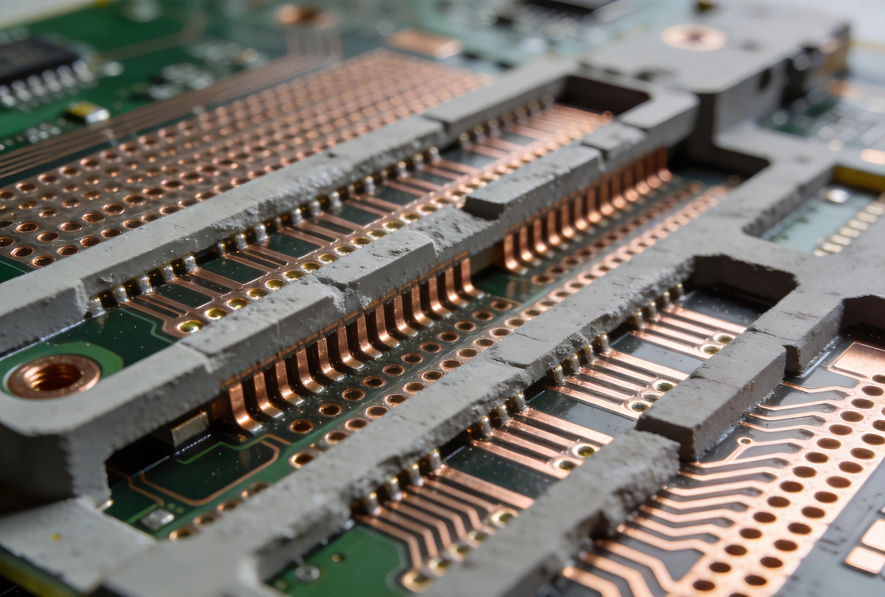
High Density Interconnect boards deliver remarkable functionality in compact packages—fine-pitch components, blind and buried vias, and dense routing that would be impossible in standard multilayer constructions. This capability comes with complexi...
https://www.high-density-interconnect-pcb.comhttps://www.high-density-interconnect-pcb.com/industrial-automation/designing-rugged-hdi-boards-for-harsh-industrial-environments/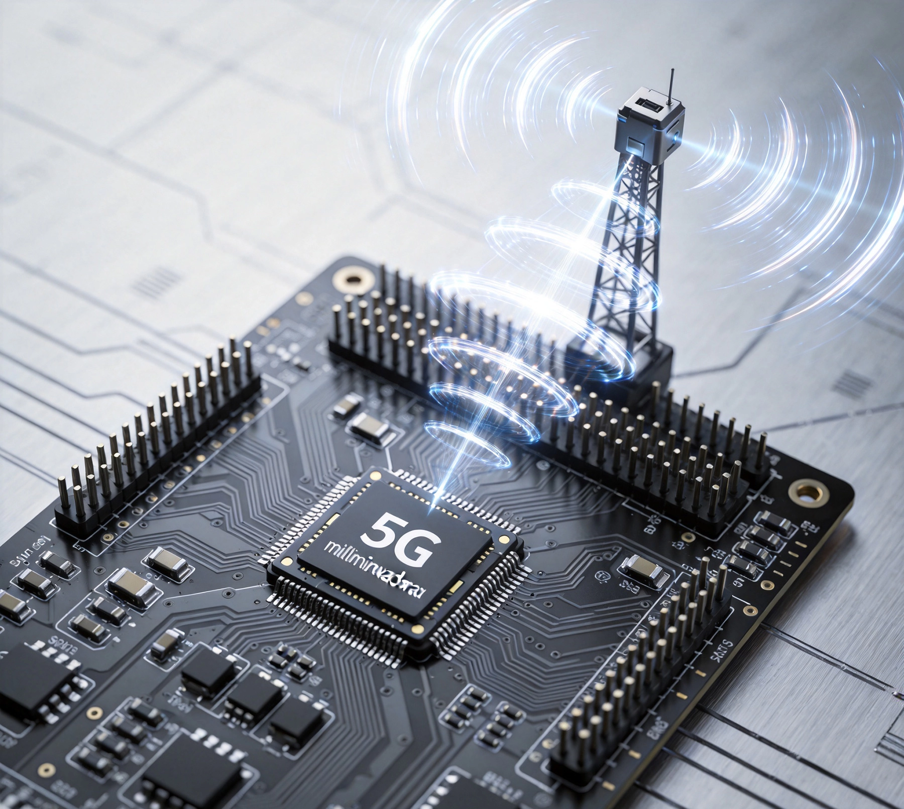
The transition to 5G millimeter wave frequencies presents PCB designers with challenges that dwarf those encountered at traditional microwave frequencies. While sub-6GHz cellular infrastructure shares many characteristics with established RF design...
https://www.high-density-interconnect-pcb.comhttps://www.high-density-interconnect-pcb.com/telecom-5g-high-speed-computing/signal-integrity-challenges-in-5g-mmwave-hdi-designs/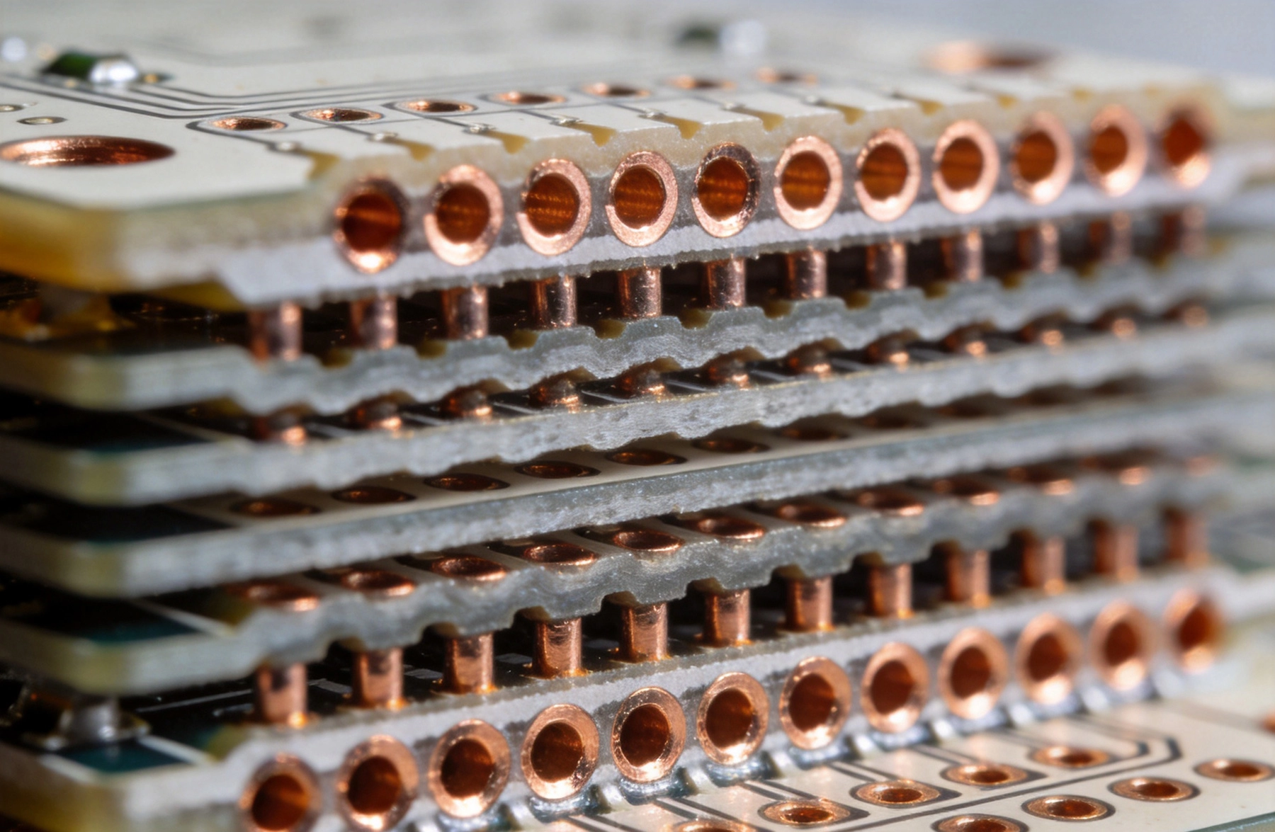
As electronics continue their relentless march toward miniaturization, high-density interconnect (HDI) technology has become standard practice rather than exotic exception. And at the heart of every HDI design lies the microvia—those laser-drilled,...
https://www.high-density-interconnect-pcb.comhttps://www.high-density-interconnect-pcb.com/hdi-pcb-design-testing/the-art-of-microvia-placement-staggered-vs-stacked-vias/