
The transition to 5G millimeter wave frequencies presents PCB designers with challenges that dwarf those encountered at traditional microwave frequencies. While sub-6GHz cellular infrastructure shares many characteristics with established RF designs, the 24GHz to 100GHz spectrum that enables multi-gigabit wireless demands Signal Integrity techniques previously reserved for advanced semiconductor packaging and aerospace applications.
High-density Interconnect (HDI) PCB technologies provide the Miniaturization and electrical performance that mmWave designs require, but they introduce their own complications. Layer counts escalate, via structures become more complex, and manufacturing tolerances that seemed acceptable at lower frequencies suddenly become critical parameters affecting yield and performance.

At 28GHz, 39GHz, or the emerging 60GHz bands, signal wavelengths shrink to single-digit millimeters. This reduction fundamentally changes how electrical energy behaves compared to lower frequencies. Transmission line dimensions that were electrically small at 5GHz become significant fractions of wavelength at mmWave frequencies, requiring careful management of geometry-dependent effects.
Skin Effect—the tendency of high-frequency current to flow near conductor surfaces—intensifies dramatically as frequency increases. At 28GHz, the effective conducting depth in copper drops to approximately 4 micrometers. This skin depth reduction increases effective resistance beyond what DC measurements predict, affecting loss budgets and thermal considerations.
Pcb Design practices developed for digital signals up to several gigabits per second often produce inadequate results at mmWave frequencies. Via stub resonances that cause minor ripples at 5Gbps become severe impedance discontinuities at 28GHz. Ground plane slots that create negligible crosstalk at lower frequencies generate substantial unwanted coupling at mmWave.
The margin for error shrinks as frequencies rise. A 10% Impedance Tolerance acceptable for 1Gbps digital signals creates unacceptable phase variation at 28GHz modulation bandwidths. Designers cannot rely on margin-based approaches that compensate for uncertainty through conservative specifications—mmWave designs require deterministic control of every parameter affecting signal propagation.
Transmission line type selection profoundly affects mmWave performance. Surface microstrip traces experience different propagation characteristics than stripline buried between reference planes. Microstrip offers easier manufacturing and Thermal Management but suffers from less predictable propagation constants due to air interface uncertainty. Stripline provides consistent propagation within solid dielectric but requires blind and Buried Vias for layer access.
Differential signaling remains essential at mmWave for the same reasons it benefits lower-frequency designs—common mode rejection, reduced radiation, and doubled signal swing. However, Differential Pair Routing becomes more sensitive at high frequencies. Even-tempered differential pairs that perform excellently at 10Gbps exhibit excessive skew at 28Gbps and beyond, requiring tighter manufacturing tolerances and more precise controlled-depth routing.
Trace width and spacing tolerances that were uncritical at lower frequencies become dominant factors at mmWave. A 0.1mm trace width variation creates negligible impedance change at 1GHz but produces measurable impedance error at 28GHz. Hdi Manufacturing processes achieve tighter tolerances than standard PCB Fabrication, but these capabilities come at premium cost and require careful specification.
Trace surface roughness affects losses at mmWave frequencies. Standard PCB copper foils with roughness exceeding 2-3 micrometers add significant attenuation at 28GHz compared to smooth electrodeposited or reversed-treated foils. Material selection and specification must account for skin depth effects that magnify surface imperfection impacts.
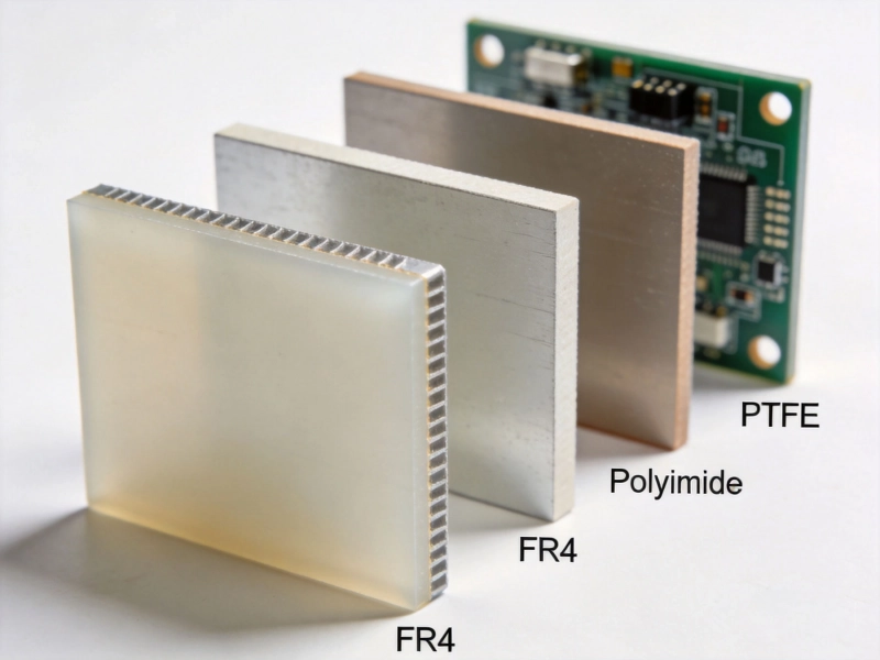
Substrate materials with consistent dielectric properties across frequency ranges become essential for mmWave designs. Standard FR-4 materials exhibit significant dispersion—meaning their effective dielectric constant varies with frequency. This dispersion complicates impedance prediction and phase matching that deterministic performance requires.
High-frequency laminates like Rogers RT/duroid, Panasonic Megtron, and similar materials offer more stable dielectric constants across wide frequency ranges. These specialized substrates cost significantly more than commodity materials but provide the property consistency that mmWave designs demand. For some applications, hybrid constructions using high-frequency materials for critical RF layers and standard materials elsewhere balance cost against performance requirements.
Every via creates impedance discontinuity in a transmission path. At lower frequencies, these discontinuities manifest as minor reactance easily absorbed within overall link budgets. At mmWave frequencies, via reactance becomes substantial relative to trace impedance, and the discontinuities they create cause measurable reflection and loss.
Via inductance depends on aspect ratio—thicker boards with longer vias exhibit higher inductance. Hdi Boards with their reduced thickness help minimize this parasitic, but even thin boards accumulating multiple layer transitions create significant discontinuities. Back-drilling removes unused via barrel sections that would otherwise create stub resonances, a technique that becomes essential rather than optional at mmWave.
mmWave modules frequently require transitions between different transmission line types or between surface traces and component contacts. These transitions create discontinuities proportional to how carefully ground references are maintained throughout the transformation. Inconsistent ground references cause mode conversion that transforms differential signals into common-mode energy and vice versa.
Ground vias placed strategically around signal vias provide return current paths that minimize inductance. The effectiveness of ground via stitching depends on spacing relative to signal wavelength—holes that would adequately ground a 5GHz signal become inadequate at 28GHz. Denser ground via arrays around mmWave routing reduce inductance but consume routing space that HDI designs often need for other purposes.
HDI constructions use Sequential Lamination to create Blind Vias—connections from surface to internal layers without penetrating the entire board thickness. These structures enable high-density routing that would be impossible with through-hole vias, but they introduce manufacturing complexity that affects electrical performance.
Blind Via aspect ratios differ from through-hole ratios, creating different capacitive and inductive characteristics. The land dimensions required for reliable manufacturing differ from standard through-hole design rules. Understanding these differences enables designs that achieve both manufacturing yield and electrical performance targets.
Crosstalk between adjacent traces increases as wavelength decreases relative to trace spacing. At 28GHz, coupling mechanisms that are purely capacitive at lower frequencies develop inductive components that complicate mitigation strategies. The transition between quasi-static coupling models and full-wave electromagnetic behavior requires more sophisticated analysis approaches.
Differential signaling continues providing crosstalk immunity, but the differential pairs themselves must be isolated from adjacent pairs. Coupling between differential pairs creates differential-to-common-mode conversion that degrades signal quality and increases electromagnetic radiation. Routing rules must account for this cross-pair coupling, not merely single-pair spacing.
Physical shielding between critical signal paths provides crosstalk reduction beyond what spacing alone achieves. Continuous ground planes between routing channels effectively isolate signals but consume routing resources. Guard traces—grounded strips placed between signal traces—offer partial isolation with less space consumption, though their effectiveness diminishes at mmWave compared to solid planes.
The choice between continuous shielding and guard trace approaches depends on routing density constraints. For extremely dense HDI designs where space prohibits extensive plane areas, guard traces provide marginal improvement over no isolation. For less constrained sections of designs, solid plane isolation between channels may be worth the routing space investment.
Accurate crosstalk prediction requires full-wave electromagnetic simulation rather than simplified analytical models. The coupling mechanisms at mmWave frequencies involve distributed effects that analytical approaches cannot capture adequately. Tools like HFSS, CST, and similar 3D electromagnetic simulators provide the accuracy that mmWave design demands.
Simulation accuracy depends on model fidelity. Approximate representations of via structures, trace geometry, and material properties introduce errors that may be acceptable at lower frequencies but become critical at mmWave. Creating simulation models that accurately represent manufactured PCBs requires close collaboration between electrical designers and manufacturing engineering to understand typical variations.
Power delivery network design becomes more challenging at mmWave frequencies. The decoupling strategies that effectively stabilize supply voltages at lower frequencies exhibit resonances and impedance peaks that permit voltage noise at mmWave frequencies. IC current transients at modulation rates approaching 1GHz can excite these resonances, creating supply noise that modulates signal paths.
Embedded capacitance in HDI constructions provides some high-frequency decoupling without discrete components. Power and ground planes separated by thin dielectric create distributed capacitance effective up to tens of gigahertz. This embedded capacitance supplements discrete decoupling capacitors but cannot replace them entirely for lower-frequency decoupling.
Power and ground planes separated by dielectric form resonant cavities that support standing waves at frequencies determined by geometry. At mmWave frequencies, these resonances fall within operating bands, potentially coupling noise from digital circuits into sensitive RF paths. Preventing this coupling requires damping these resonances through strategic placement of resistive materials or termination networks.
Slot antennas formed by plane discontinuities radiate energy that creates both electromagnetic compatibility problems and Signal Integrity degradation. These slots become more significant at mmWave where they align with operating frequencies. Careful plane design that avoids slot formation or strategic shielding over slots addresses this issue.
Hdi Boards with many Sequential Lamination cycles accumulate registration errors as each layer is added. The acceptable tolerance for layer-to-layer alignment shrinks at mmWave frequencies where trace widths and spacings are smaller. Misregistration between layers creates impedance variations and coupling asymmetries that affect performance.
Manufacturers have improved registration capabilities through better equipment, enhanced materials, and statistical process control that identifies drift before it creates out-of-specification product. However, these capabilities come at cost premiums that affect board pricing. Designers must specify tolerances achievable at target cost points rather than idealized requirements.
Time-domain reflectometry validates trace impedance during manufacturing, but the measurement bandwidth determines what features can be detected. Standard Tdr equipment with nanosecond rise times may not adequately characterize impedance variations at mmWave frequencies where these variations occur over distances shorter than the effective spatial resolution.
Network analyzer measurements in the frequency domain provide more accurate characterization of transmission line performance at mmWave frequencies. These measurements capture Insertion Loss, return loss, and phase response that Tdr cannot directly measure. The tradeoff involves higher equipment cost and longer test times that affect manufacturing economics.
mmWave characterization often requires measurement approaches that minimize fixturing effects. Probe stations with calibrated millimeter-wave probes enable measurements directly at device contacts, removing transmission line and connector effects from the measurement. These techniques originated in semiconductor testing but apply increasingly to high-performance PCB characterization.
Calibration standards for mmWave measurement require careful attention. The calibration methods appropriate at lower frequencies introduce errors that become significant at 28GHz and beyond. Understanding calibration limits and residual errors enables realistic assessment of measurement uncertainty.
Process capability of manufacturing parameters directly affects yield at mmWave frequencies. Impedance Tolerance, spacing uniformity, and registration accuracy all follow statistical distributions. Understanding these distributions enables yield prediction and helps identify which parameters most affect final performance.
Monte Carlo simulation incorporating manufacturing variations predicts performance distributions before fabrication. This prediction enables designers to understand which variations most affect their circuits and which can be tolerated without performance impact. Production testing can then focus on parameters with greatest performance sensitivity.
Successful mmWave HDI designs require collaboration between electrical and mechanical engineering from project inception. The mechanical constraints of packaging, Thermal Management, and manufacturing affect electrical decisions that must be made early. Waiting for mechanical design completion before beginning electrical design creates schedules that cannot recover.
Sharing models between electrical simulation and mechanical analysis tools enables optimization across domains. Thermal simulations that account for power distribution and RF heating inform electrical design, while electrical parameters constrain mechanical arrangements. This integration requires process and tooling investments but produces better products faster.
mmWave designs benefit from staged validation that identifies issues progressively. Initial prototypes using representative materials verify basic electrical concepts before committing to final material choices. Secondary prototypes incorporating manufacturing representative processes verify producibility. Production validation confirms that manufactured assemblies meet specifications.
Test vehicle designs that isolate specific design elements enable targeted validation without complex full assemblies. Transmission line test structures, via transition measurements, and coupling characterization vehicles provide data that supports analysis of more complex circuits. These investments in characterization improve confidence when final designs enter production.
5G mmWave implementations typically occupy spectrum from 24GHz to 100GHz. The 28GHz and 39GHz bands are most widely deployed for initial 5G services. Emerging allocations extend toward 60GHz and 71GHz as spectrum regulators expand available bandwidth.
HDI enables Miniaturization that reduces parasitic effects from longer traces and larger vias. The thin dielectrics between dense metal layers provide controlled impedance with shorter via lengths that reduce inductance. These characteristics align well with mmWave design requirements for compact, low-loss interconnections.
Practical trace lengths depend on loss budgets and signal quality requirements. At 28GHz with high-quality laminates, traces up to 100-200mm may be acceptable for some applications. Higher frequencies or lossy materials require shorter traces. Active circuits may be preferable to long transmission lines when practical.
Manufacturing test uses time-domain reflectometry for impedance verification and network analyzers for Insertion Loss and return loss characterization. Test coupons representing critical transmission line types are fabricated alongside production boards for destructive and non-destructive verification.
High-frequency laminates from manufacturers like Rogers, Panasonic, and Isola provide consistent dielectric properties across mmWave frequencies. Material selection depends on specific frequency bands, loss requirements, thermal management needs, and cost constraints. Hybrid constructions may balance performance and cost.
Standard manufacturing can achieve limited mmWave performance depending on frequency and performance requirements. For many 5G applications, standard processes with tight process control and careful specification can achieve adequate results. Extremely demanding applications require specialized high-frequency manufacturing with correspondingly higher costs.
Signal integrity at 5G mmWave frequencies demands attention to details that lower-frequency designs can ignore. Transmission line Impedance Control, via transitions, crosstalk management, and manufacturing variation all require systematic consideration that Traditional Pcb design approaches do not address. Hdi Technology provides the miniaturization that mmWave designs need but introduces manufacturing complexity that must be understood and managed.
Successful mmWave HDI design requires simulation accuracy that matches manufacturing capabilities, testing approaches that validate performance at operating frequencies, and close collaboration between electrical, mechanical, and manufacturing engineering. The investment in these capabilities repays through products that achieve the performance that 5G applications require.
As 5G networks expand and new spectrum allocations push frequencies even higher, the signal integrity techniques that work at 28GHz will evolve further. Designers who master mmWave HDI fundamentals now position themselves for success as the industry continues its trajectory toward ever higher frequencies and more demanding performance requirements.
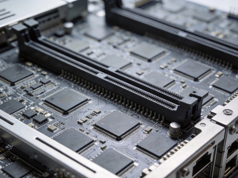
How HDI Technology Supports PCIe Gen5 and Gen6 ComputingSeptember/15/2026
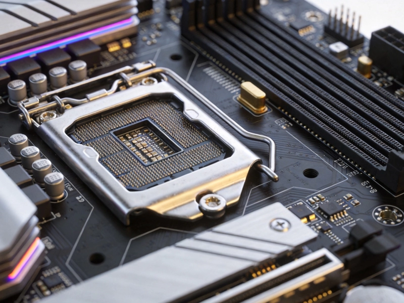
HDI Solutions for High-Performance Gaming Consoles and LaptopsSeptember/10/2026

Enabling 5G Base Stations with Low-Loss HDI PCB MaterialsJune/27/2026

The Role of HDI in High-Speed Server and Data Center HardwareJuly/18/2026
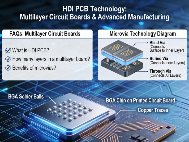
Top 10 Frequently Asked Questions About HDI PCB TechnologyMay/28/2026
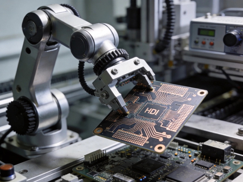
The Role of HDI in Robotics and Motion Control SystemsAugust/10/2026
Selecting the Right Dielectric Materials for High-Performance HDI PCBsMay/28/2026
Best Practices for BGA Fanout and Routing in HDI LayoutsJuly/07/2026