
Modern data centers face unprecedented demands as cloud computing, artificial intelligence, and streaming services generate exponential growth in data traffic. The servers and networking equipment that power this digital infrastructure must deliver higher performance within the same or smaller physical footprints, pushing conventional PCB technologies toward their limits. High-density Interconnect (HDI) technology has emerged as the enabling foundation that makes next-generation server and Data Center Hardware possible.
HDI PCBs provide the routing density, electrical performance, and Miniaturization that data center equipment requires. From blade servers densely packed with processors to switching ASICs operating at 400Gbps, Hdi Technology appears throughout modern computing infrastructure. Understanding how HDI enables these systems helps engineers appreciate the Pcb Design decisions that affect server performance and reliability.

Data center operators face constant pressure to increase computing capacity without expanding physical infrastructure. Rack space remains finite, power and cooling capacities are expensive to upgrade, and floor space commands premium rents in commercial data centers. These constraints drive demand for server hardware that delivers maximum performance within minimum volume.
Traditional Pcb technology using through-hole vias and standard trace geometries requires substantial board area for routing connections between components. As processor pin counts increase and package sizes shrink, the routing density achievable with conventional approaches becomes limiting. Hdi Technology breaks through these limitations by enabling more connections in less space through Microvia structures and finer trace geometries.
AI and machine learning workloads place extreme demands on server hardware, requiring multiple high-bandwidth processors communicating at speeds exceeding 100Gbps. Memory interfaces for these systems demand hundreds of signal connections operating at 6.4Gbps or higher. Meeting these requirements while maintaining Signal Integrity requires controlled impedance traces with precise routing geometry that HDI technology enables.
The transition to PCIe 5.0 and emerging PCIe 6.0 standards doubles data rates every few years, pushing signaling speeds toward 32GT/s and beyond. At these frequencies, trace length tolerances and Impedance Control become critical for reliable operation. Hdi Manufacturing processes provide the dimensional precision necessary for consistent electrical performance across high-volume production of server hardware.
HDI PCBs employ Microvias with diameters typically ranging from 100 to 150 microns compared to 300 microns or more for standard through-hole vias. These smaller vias consume significantly less board area while providing interlayer connections. The routing channels freed by Microvia Miniaturization enable more traces between components and more component density on the board.
Stacked microvia constructions, where one microvia lands directly on the landing pad of the next layer, achieve the highest routing density. This approach enables escape routing from fine-pitch BGA packages where the pad spacing is too tight for conventional fan-out patterns. Server processors and ASICs with thousands of signal connections rely on this HDI capability to route signals from package to board.
HDI constructions typically employ a core substrate with additional build-up layers on one or both surfaces. Each build-up cycle adds dielectric thickness and copper pattern layers, increasing total layer count without the complexity of true multilayer construction. A typical server HDI board might use a simple 4-8 layer core with 2-4 build-up layers on each surface.
Build-up layers provide the routing flexibility necessary for high-speed signal fan-out from advanced packages. Ground and power planes in the core establish reference impedance for controlled impedance traces. The build-up layers route signals with controlled geometry optimized for high-frequency performance. This layer architecture balances electrical performance, manufacturing complexity, and cost effectively.
Server processors from Intel, AMD, and ARM employ HDI substrates that provide interconnections between the silicon die and the processor package. These substrates, often called interposers or build-up substrates, use HDI construction to route signals from fine-pitch die-level interconnections to the larger pitch of the package ball grid array. The signal density required for modern server processors makes HDI substrates essential.
Package-level HDI substrates typically employ very fine geometries—traces of 15-20 microns width with corresponding spacing. These substrates are manufactured as separate components that are attached to the processor die through flip-chip bonding. The substrate manufacturer specializes in HDI technology, while the server board manufacturer focuses on system-level interconnect.
Network switches that move terabits of data per second across data center networks rely heavily on HDI technology. These ASICs, controlling 32, 64, or more high-speed ports, require massive fan-out from their BGA packages. The routing density necessary for 400Gbps and emerging 800Gbps interfaces would be impossible with conventional Pcb Technology.
Switch boards typically employ high-layer-count HDI constructions with numerous build-up layers to accommodate the routing complexity. Controlled impedance traces for 25Gbps, 50Gbps, and 100Gbps lanes must maintain consistent geometry throughout their runs. The manufacturing precision of HDI processes ensures that impedance targets are met across production volumes of thousands of boards.
Server memory subsystems present significant routing challenges due to the number of signals involved and the speed requirements. DDR5 interfaces operating at 6.4Gbps require controlled impedance traces with tight length matching tolerances. The channel topology, whether point-to-point or branched, affects routing complexity and board area requirements.
HDI technology enables high-density memory interface routing on server motherboards and add-in cards. The ability to route many matched-length traces in tight spaces makes memory interfaces practical at the speeds that modern servers require. Advanced memory architectures like HBM (High Bandwidth Memory) employ HDI interposers that connect memory stacks to processing elements.
High-speed server signals require controlled impedance traces that maintain consistent 50-ohm single-ended or 100-ohm Differential Impedance. Hdi Manufacturing processes provide the dimensional control necessary for achieving these targets across production volumes. Trace width, thickness, dielectric height, and material properties must all be held within tight tolerances.
The thinner dielectric layers typical of HDI construction enable controlled impedance traces with narrower widths than conventional boards. This dimensional scaling supports the fine pitch routing necessary for high-density server components. Manufacturing process controls verify impedance through coupon testing and statistical process control that maintains performance within specification.
Vias introduce discontinuities that affect signal quality at high speeds. The capacitive and inductive effects of via structures can degrade signal transitions and create reflections that limit bandwidth. HDI Microvias, with their smaller pad diameters and shorter stub lengths, create fewer discontinuities than conventional through-hole vias.
Back-drilling removes unused via stubs on critical high-speed signals, eliminating resonant stub effects that would otherwise limit bandwidth. This technique is particularly valuable for differential pairs where both traces must exhibit similar electrical length and characteristic. The combination of Microvia Technology and back-drilling optimization enables high-speed channels that meet demanding loss budgets.
At 25Gbps and beyond, conductor and dielectric losses accumulate significantly over routing distances. Low-loss Pcb Materials reduce signal attenuation but increase cost compared to standard laminates. The selection of materials balances electrical performance against budget constraints for different signal classes on the same board.
Critical high-speed lanes may route on premium Low-loss Materials while lower-speed signals use standard materials. This material segmentation optimizes cost without compromising performance for the signals that matter most. Material data sheets specify Insertion Loss characteristics that enable accurate loss budgeting during design.
Server processors and ASICs dissipate hundreds of watts within their packages, creating concentrated heat sources that stress Thermal Management systems. The high circuit density of Hdi Boards can either help or hinder heat removal depending on how thermal paths are designed. The proximity of components enabled by HDI miniaturization can create thermal interaction that complicates cooling system design.
Hdi Boards themselves contribute to thermal challenges because the thin dielectric layers have limited Thermal Conductivity. Heat generated in inner layers must conduct through multiple interfaces to reach heat spreaders or cooling solutions on outer surfaces. Thermal via constructions and metal core substrates address these limitations for high-power applications.
Thermal Vias provide low-resistance heat conduction paths from heat-generating components to heat spreaders or the board edge. These vias, typically unfilled but often tented with solder mask, connect surface pads to inner planes or through the entire board thickness. Their placement near hot components reduces junction temperatures that would otherwise limit processor performance.
Metal core HDI constructions embed copper or aluminum cores within the PCB stack-up to provide efficient heat spreading. These constructions sacrifice some routing flexibility to gain Thermal Performance, making them suitable for dedicated power delivery modules rather than fully routing-intensive boards. The Thermal Conductivity of metal core materials exceeds standard dielectrics by orders of magnitude.
The interface between HDI boards and cooling solutions requires careful design to ensure reliable heat transfer. Thermal interface materials (TIM) fill microscopic gaps between component packages and heat sinks, providing paths for heat flow. The selection of TIM materials and application methods affects thermal resistance that ultimately determines component junction temperature.
Ball grid array packages used on server processors distribute heat from the die across the package substrate to many solder balls. These balls, when soldered to the board, conduct heat from the package to internal planes that distribute it across the board. The thermal resistance of this path must be included in system-level thermal models that predict operating temperatures.
HDI manufacturing involves more process steps than conventional PCB Fabrication, creating more opportunities for yield loss. Each build-up layer adds process complexity that must be controlled to achieve acceptable final board yields. The fine geometries of HDI traces and microvias require precise process control that demands sophisticated manufacturing equipment and experienced personnel.
Quality verification for HDI server boards includes Automated Optical Inspection, electrical testing, and sometimes X-ray analysis for hidden features. The cost of detecting and preventing defects drives part of the higher manufacturing cost compared to conventional boards. Quality systems must balance inspection rigor against the cost that extensive testing adds to each board.
Data Center Hardware operates continuously for years between maintenance windows, with reliability requirements measured in mean time between failures. HDI boards in this environment must survive temperature cycling from server on-off cycles, vibration from cooling fans, and humidity variations from environmental control systems. The manufacturing quality of HDI boards directly affects field reliability.
Thermal cycling reliability testing validates that HDI microvias and plated-through holes survive expected temperature excursions without cracking. Accelerated life testing compresses time to failure so that design weaknesses are found before production boards reach data centers. Industry standards like IPC provide test methods and acceptance criteria that define minimum reliability requirements.
Data center networks continue pushing toward 800Gbps and 1.6Tbps aggregate speeds to accommodate growing traffic demands. These higher speeds will require even finer HDI geometries and more sophisticated materials to maintain Signal Integrity. New PCB technologies including ultra-Low-loss Materials and finer line/spacing capabilities are under development to meet these requirements.
Co-packaged optics, where optical engines are integrated with switching ASICs, represents a significant architectural shift that will affect Pcb Design. The optical interfaces require precise alignment and Thermal Management that challenge conventional PCB approaches. HDI technology will likely play a role in these co-packaged designs, though specific implementations remain under development.
The semiconductor industry is transitioning from monolithic processor designs to chiplet architectures that combine multiple smaller chips in a single package. This approach enables mixing different process technologies and scaling individual chiplets independently. HDI substrates will be essential for routing the massive number of interconnections between chiplets in these advanced packages.
Organic substrates using HDI-like constructions are competing with silicon interposers for chiplet integration applications. The lower cost and larger panel sizes of organic substrates make them attractive for high-volume production despite some performance limitations compared to silicon. This trend will drive continued evolution of HDI technology for packaging applications beyond traditional board-level electronics.
HDI technology has become indispensable for high-speed server and data center hardware, enabling the routing density and electrical performance that modern computing requires. From processor packages to switching ASICs to memory interfaces, HDI constructions appear throughout server hardware that powers cloud computing and AI workloads. The microvia structures, build-up layer architectures, and precise manufacturing that define HDI technology make next-generation performance possible.
Signal integrity and thermal management remain the primary challenges for HDI in server applications. As data rates continue increasing and power densities grow, HDI board designers must optimize trace geometry, via structures, and materials to maintain reliable performance. The evolution of HDI technology will track the demands of data center hardware, with new capabilities enabling the next generation of computing infrastructure.
The investment in HDI manufacturing capability represents a significant commitment that limits competition in high-performance server board production. As data center operators demand more computing capacity, the HDI technology supply chain will continue expanding to meet demand. Understanding HDI's role in server hardware helps engineers appreciate the PCB innovations that make modern data centers possible.
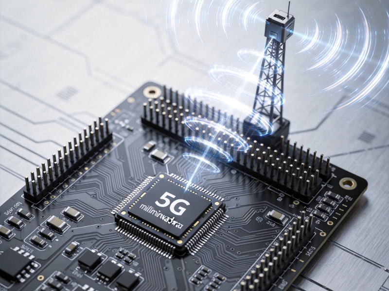
Signal Integrity Challenges in 5G mmWave HDI DesignsAugust/08/2026
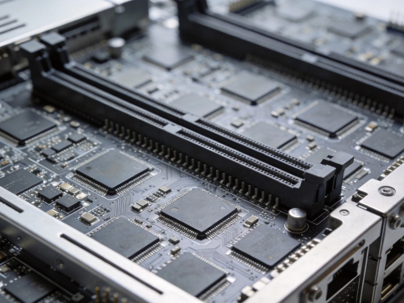
How HDI Technology Supports PCIe Gen5 and Gen6 ComputingSeptember/15/2026
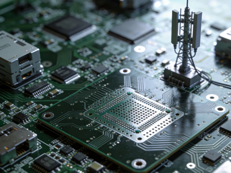
Enabling 5G Base Stations with Low-Loss HDI PCB MaterialsJune/27/2026
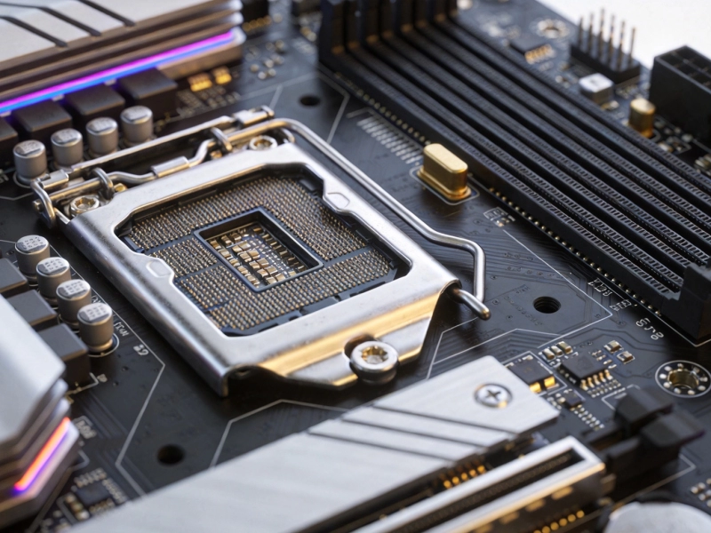
HDI Solutions for High-Performance Gaming Consoles and LaptopsSeptember/10/2026
Reliability Challenges of Via-in-Pad Plating Filled (VIPPO) TechnologySeptember/30/2026
High-Reliability HDI Solutions for PLCs and Motor DrivesSeptember/16/2026
Understanding Sequential Lamination in Multi-Step HDI BoardsJuly/03/2026
The Evolution of PCB Technology: From Standard Multilayer to HDIJune/02/2026