Open Nav

Power inverter designers constantly chasing efficiency improvements increasingly turn to High-density Interconnect technology to shrink footprints while pushing power density higher. The promise of HDI—Micro Vias, finer trace geometries, and buried capacitance—compels engineers to reconsider traditional board architectures. But integrating HDI into high-efficiency power conversion systems introduces complications that pure digital designers never encounter. Thermal Management becomes more challenging when power devices crowd beneath control circuitry. Switching noise couples into sensitive measurement paths through shared capacitance. Manufacturing costs multiply faster than density gains suggest. Before committing your next power inverter project to HDI, understanding these interconnected challenges determines whether the technology delivers on its promise or creates problems worse than the ones you solved.
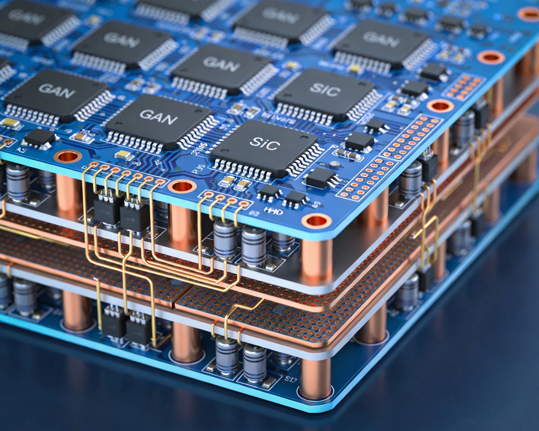
High-efficiency power inverters already push silicon limits—gallium nitride and silicon carbide devices switching at megahertz frequencies to minimize magnetic component sizes. HDI seems like a natural companion, enabling dense gate drive circuitry and compact control loops. Yet efficiency itself creates paradoxes when combined with HDI integration.
Modern wide-bandgap inverters achieve 98%+ efficiency, which sounds impressive until you calculate absolute losses. A 10kW inverter at 98% efficiency dissipates 200 watts as heat. In a traditional design, this heat spreads across substantial copper area and Thermal Vias. HDI integration crowds power components into tighter spaces, concentrating dissipation into smaller areas that thermal relief structures cannot adequately address.
The Thermal Conductivity of thin dielectric layers in HDI stackups—often below 0.5W/mK for standard prepreg—creates thermal resistance far exceeding thick FR-4 cores in traditional laminates. Heat flowing from power devices through Micro Via arrays encounters cumulative resistance that elevates junction temperatures dangerously.
Silicon carbide and gallium nitride devices tolerate higher temperatures than silicon, but their performance degrades significantly at elevated junction temperatures. SiC MOSFETs lose approximately 20% of on-resistance at 150°C compared to 25°C operation. GaN devices show similar sensitivity, plus derating requirements for threshold voltage stability over lifetime.
Thermal Simulation models built for Traditional Pcb structures may underestimate temperatures in HDI designs due to inaccurate thermal property assumptions for thin dielectrics. Designers must either over-verify with generous margins or invest in thermal characterization of specific HDI stackups—often unavailable from fabricators without extensive testing.
Power inverters require precise control loops measuring current and voltage feedback while generating switching waveforms. HDI integration affects Signal Integrity in ways that complicate these measurements.
Fast-switching GaN and SiC devices generate voltage transients exceeding 100V/ns during hard switching events. These rapidly changing potentials couple into nearby signal traces through multiple mechanisms: capacitive coupling through adjacent dielectrics, common impedance coupling through shared power/ground references, and radiated coupling across air gaps.
HDI designs with layered Micro Via structures create complex capacitance networks between power switching nodes and sensitive measurement circuits. Buried capacitance layers intended to decouple power rail noise may inadvertently couple switching transients into signal planes running in adjacent layers. The dense routing that makes HDI attractive simultaneously makes identifying coupling paths more difficult.
High-current power inverter ground references experience significant voltage drops during switching transients. The dV/dt of SiC switching creates displacement currents through parasitic capacitance to PCB ground planes, injecting noise into ostensibly quiet ground references used by analog control circuits.
HDI stackups with multiple ground plane layers may seem to offer better grounding than two-layer traditional designs, but plane segmentation required to accommodate dense routing fragments the ground reference. Current return paths must navigate through stitching vias and plane gaps, creating inductances that become problematic at the nanosecond timescales of wide-bandgap switching.
Precision current sensing in high-efficiency inverters uses either shunt resistors with differential amplifiers or Hall-effect sensors. Shunt resistor placement in HDI power stages must balance proximity to switching nodes—introducing noise—against distance that adds parasitic inductance and degrades high-frequency measurement bandwidth.
Layout symmetry critical for current sensing in interleaved converters becomes harder to achieve when routing density compresses geometry. Mismatched sense trace lengths and varying via counts create offset errors that compound across multiple phases, undermining the balance essential for optimal interleaving performance.
Hdi Manufacturing processes involve more steps, tighter tolerances, and higher defect rates than standard multilayer fabrication. Power inverter applications stress HDI capabilities in ways that reveal these limitations.
Micro Vias in HDI designs experience coefficient of thermal expansion mismatches between copper barrel and surrounding dielectric. Standard HDI constructions using laser-ablated micro vias with thin dielectric volumes create stress concentrations during thermal cycling. Power inverter thermal environments—ranging from cold outdoor installations to hot industrial enclosures—accelerate micro via fatigue.
IPC Class 3 requirements for industrial Power Electronics specify acceptance criteria for micro via integrity that many HDI fabricators struggle to consistently meet. The aspect ratios of micro vias—typically 0.5:1 to 1:1 compared to 3:1 or higher for standard PTH—limit plating thickness achievable in barrel walls, potentially creating reliability risks for high-reliability applications.
Thermal Vias connecting power device pads to internal planes in HDI designs create assembly challenges. Standard thermal via arrays using 0.3mm diameter vias with 0.8mm pitch create substantial solder voiding risk under bottom-thermal-pad packages. Void percentages exceeding IPC 3% thresholds for Class 3 applications may occur despite standard paste stencil practices.
The Sequential Lamination required for complex HDI stackups—often five or more buildup cycles—creates cumulative registration challenges. Thermal via arrays may not align perfectly with buried planes and routing layers, creating thermal resistance variations across pad areas. Fabricators cannot guarantee thermal uniformity across large power pads at HDI tolerances.
Gate drive circuits for wide-bandgap devices require controlled impedance traces for signals traveling from control processors to gate drivers. HDI constructions with thin dielectrics between signal and reference planes create impedance values sensitive to manufacturing variations in dielectric thickness and copper roughness.
Standard impedance tolerances of ±10% may be insufficient for some gate drive applications requiring precise timing between high-side and low-side signals. HDI microstrip and stripline constructions with thin dielectrics amplify the impedance sensitivity to plasma etching variations, potentially requiring tighter tolerances that fabricators price at premiums.
HDI promises cost savings through board size reduction—smaller boards require less material and fit more units per panel. Reality involves manufacturing cost multipliers that often exceed size savings.
HDI fabrication involves Sequential Lamination cycles, Laser Via formation, and additional plating steps that scale costs faster than density increases. A typical HDI board with three buildup layers may cost 2-4x more per square inch than an equivalent two-layer design, even when accounting for size reduction benefits.
Power inverter applications requiring heavy copper—2oz or 3oz outer layers for power dissipation—create additional complexity. HDI fabricators typically optimize for thin traces and micro vias, working with 1oz or 0.5oz copper that simplifies laser ablation and plating. Heavy copper HDI requires specialized processing that further elevates costs and potentially reduces yield.
Complex HDI stackups exhibit lower manufacturing yields than standard multilayer boards due to more processing steps and tighter tolerances. Fabricators price HDI work with yield loss assumptions that raise quoted prices beyond raw material and processing costs.
Power inverter defects have consequences beyond board scrap. Field failures of Power Electronics may damage connected systems or create safety hazards. Purchasing Hdi Boards from suppliers with immature HDI processes creates quality risks that may not appear during initial qualification but emerge during production scaling or in-field operation.
Successfully integrating HDI into power inverters requires design approaches that acknowledge HDI limitations while exploiting its genuine advantages.
Keep power switching nodes physically separated from HDI-dense control sections. Use traditional multilayer regions for power stages while reserving HDI for control circuits. This hybrid approach preserves Thermal Management capability while capturing density benefits where density actually matters.
Interface between HDI control sections and power stages through controlled-impedance transition structures that minimize parasitics and provide clean signal handoff. The additional routing area for these transitions often pays for itself through improved Signal Integrity and reduced debug cycles.
Design separate ground islands for power switching, gate drive, and sensitive analog measurement circuits. Connect islands at single points to control noise coupling while maintaining ground reference integrity for each domain. HDI routing flexibility enables ground segmentation that would be impractical in traditional designs.
Stitching vias connecting ground planes must be placed deliberately rather than automatically added by design software. Over-stitching creates unnecessary inductance loops; insufficient stitching leaves ground islands floating relative to each other. Careful placement following signal current return paths optimizes ground connections.
Use thermal relief spokes only where absolutely necessary for soldering. For boards assembled with reflow or vapor phase processes, consider full thermal connection on heavy copper HDI designs despite the manufacturing implications. Pre-heating capabilities in modern assembly equipment handle direct thermal connections without solderability concerns.
If wave soldering remains necessary for through-hole components, thermal relief patterns should be widened beyond standard dimensions when carrying high currents. Wider spokes at 0.5-0.8mm handle more current while still providing some thermal separation for wave soldering compatibility.
HDI may not always be the right solution. Understanding alternatives helps frame when HDI integration makes sense versus when simpler approaches deliver better outcomes.
Modern 4-6 layer multilayer boards with standard PTH technology achieve remarkable density when routing is optimized. Blind and Buried Vias in traditional constructions provide density without full HDI complexity and cost escalation. Sequential lamination for two or three buildups costs far less than full HDI while capturing most density benefits.
Instead of integrating everything onto one HDI board, consider modular architectures with specialized sub-assemblies. Gate drive transformers and current sensors can be discrete modules connected to main control boards through controlled-impedance connectors. This approach separates thermal, mechanical, and electrical concerns while enabling optimization of each domain.
Some inverter manufacturers use flexible circuits to connect gate drivers directly to power modules, eliminating gate drive PCB routing entirely for the highest-speed signals. This approach trades interconnection complexity for signal integrity improvements that may justify the additional assembly steps.
Evaluating HDI integration for power inverter applications requires honest assessment of whether density benefits justify the additional complexity and cost.
Applications with severe space constraints—vehicle-mounted inverters, aerospace power systems, portable equipment—where board volume reduction outweighs manufacturing cost increases benefit from HDI integration. Systems requiring many parallel gate drive channels benefit from HDI routing density that would require impractically large boards otherwise.
Designs already using GaN devices with their inherent high-frequency capability may need HDI to route the resulting high-bandwidth signals without excessive parasitics. When the technology enabling performance improvement also demands HDI integration, the trade-off becomes clearer.
Industrial inverters operating in harsh thermal environments with long lifetime requirements may be better served by traditional technologies. The reliability margin sacrificed by HDI thermal challenges may not be worth the density benefits. Cost-sensitive consumer products with short development cycles may similarly avoid HDI's longer qualification and debugging processes.
Designs approaching thermal limits already—where efficiency improvements require aggressive thermal management—should avoid HDI until fabricators develop HDI constructions with thermal conductivities approaching traditional materials. Current HDI Thermal Performance lags far behind what power electronics require for comfortable design margins.
HDI integration into high-efficiency power inverters delivers genuine density benefits alongside genuine integration challenges. Thermal management, signal integrity, manufacturing complexity, and cost structures each present obstacles requiring deliberate design attention. The technology serves some applications well while creating problems for others.
Before committing to HDI, honestly assess whether your application genuinely needs the density HDI provides. Space-constrained applications with GaN-based designs and controlled manufacturing environments may justify the integration effort. Traditional applications without severe space constraints likely benefit from conventional multilayer approaches or modular architectures.
If you proceed with HDI power inverter integration, allocate time and budget for thermal validation beyond standard simulation. Characterize actual Hdi Stackup thermal properties rather than relying on datasheet values. Verify signal integrity through bench testing under representative switching conditions, not just simulation. Accept that debugging HDI power electronics requires patience and iteration.
The power electronics industry will continue pushing integration higher. Hdi Technology improves incrementally, fabricators develop power-optimized constructions, and design methodologies mature. Today's challenging integration may become tomorrow's straightforward implementation. Track technology developments and revisit HDI assessments as the ecosystem evolves.
Your application requirements should drive technology selection, not technology availability. HDI integration may or may not serve your specific needs. Make that determination with clear understanding of the challenges rather than optimistic assumptions about technology capabilities.
The Role of HDI in Smart Grid and Energy Storage SystemsAugust/06/2026
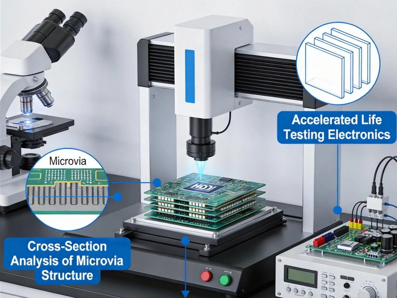
Key Factors Influencing the Long-Term Reliability of HDI PCBsMay/28/2026
How HDI PCBs Power the Next Generation of SmartphonesJune/17/2026
How HDI Technology Enables the Miniaturization of Modern ElectronicsSeptember/20/2026
HDI Applications in Advanced Battery Management Systems (BMS)June/18/2026
The Importance of Electrical Testing for Microvia ReliabilityJuly/09/2026
Why IoT Sensors Rely on High-Density Interconnect TechnologyOctober/13/2026
The Art of Microvia Placement: Staggered vs. Stacked ViasSeptember/24/2026