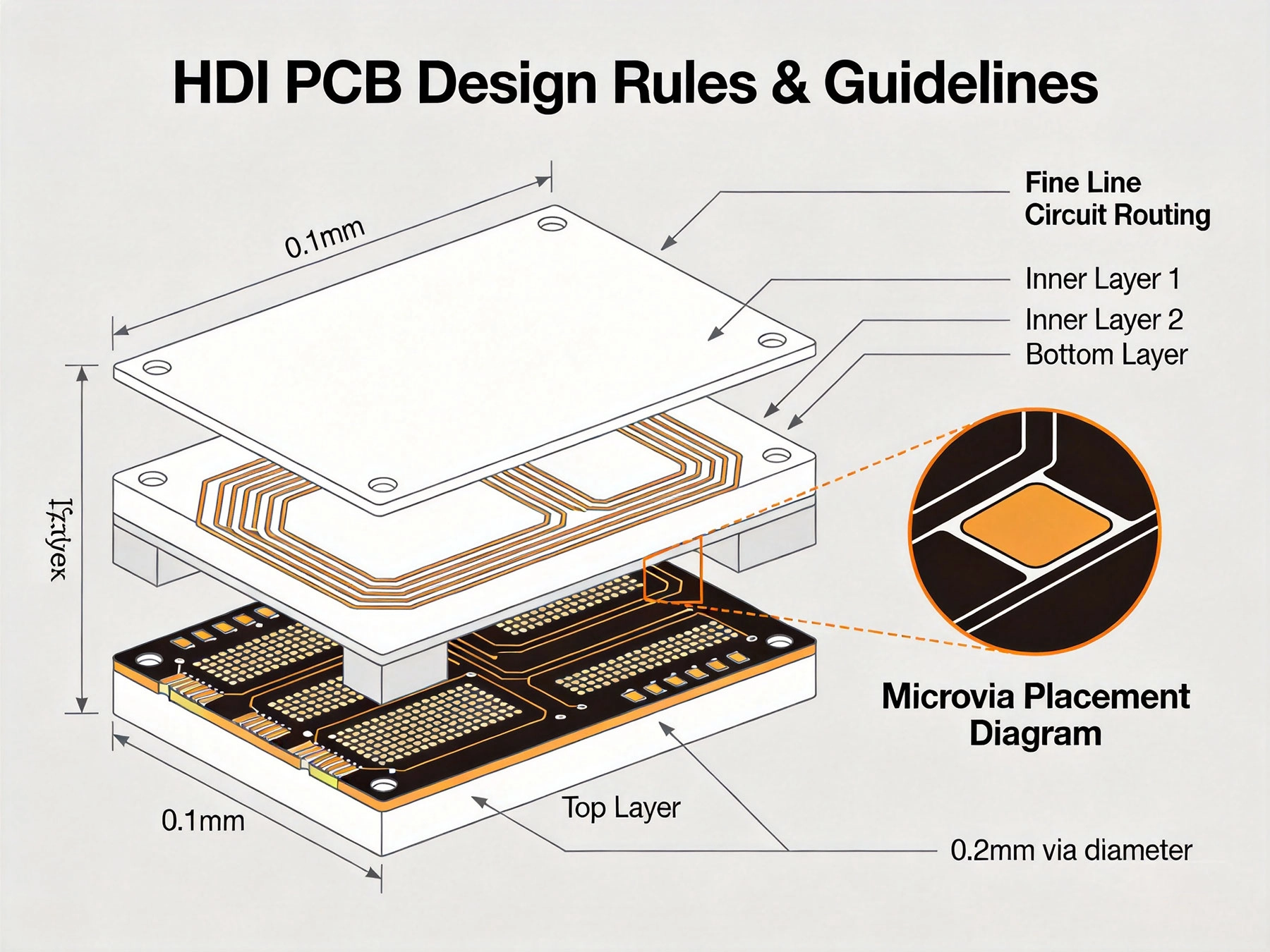
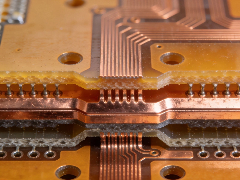
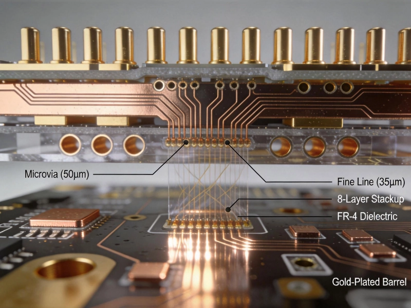
Designing an Hdi Pcb is fundamentally different from designing a conventional multilayer board. The rules you learned for standard PCB layout — things like trace widths, via sizes, and clearance requirements — don't always apply when you're working with 50-micron traces, laser-drilled Microvias, and Sequential Lamination stackups. Get these rules wrong, and you end up with boards that are expensive to manufacture, have low yields, or fail prematurely in the field. Get them right, and you unlock the full potential of Hdi Technology: maximum density, optimal electrical performance, and reliable production at scale. This guide covers every essential Hdi Pcb design rule, from the basics that beginners need to master to the advanced techniques that experts rely on.

Understanding HDI Design Complexity: Why Rules Matter More
Before diving into specific rules, it's important to understand why Hdi Pcb Design demands more rigorous adherence to design guidelines than conventional boards. In a standard 4-layer PCB, a design rule violation might cause a manufacturing headache or a minor yield reduction. In an any-layer HDI board with 12 routing layers and thousands of Microvias, the same violation can cascade into catastrophic failure.
The reason is density. Hdi Boards pack the same functionality — sometimes more — into a fraction of the board area. This means the consequences of errors are magnified. A misaligned via that would be a minor defect on a large trace becomes a killer defect when it sits between two fine-pitch components. A thermal stress that causes a hairline crack in a conventional board becomes a field failure in an HDI board because there's no redundant routing to carry the signal around the failure point.
The HDI Design Challenge in Numbers
- Trace widths in HDI can be as small as 40-50 microns (compared to 100-150 microns in standard boards)
- Microvia diameters of 50-150 microns (compared to 200-300 microns for standard through-holes)
- Registration tolerances of ±30-50 microns (compared to ±75-100 microns for standard boards)
- Layer counts that can reach 14-20 layers in advanced any-layer designs
Part 1: Fundamental HDI Design Rules for Beginners
These rules form the foundation of Hdi Pcb Design. If you're new to HDI, master these before attempting more complex designs.
Beginner Rule 1: Choose the Right HDI Configuration
Your first and most fundamental decision is selecting the HDI configuration that matches your density and cost requirements. Don't over-specify — a 1-N-1 board costs significantly less than an any-layer board, and for many applications it's more than sufficient.
Configuration Guidelines:
- 1-N-1: Use for moderate density needs. Good for mid-range smartphones, tablets, and industrial controls. Minimum Microvia: 100 microns. Layer reduction potential: 20-30% compared to equivalent through-hole design.
- 2-N-2: Use for high density requirements. Suitable for flagship smartphones, medical devices, and networking equipment. Minimum microvia: 75 microns. Layer reduction potential: 30-40%.
- Any Layer: Use only when maximum density is essential. Found in flagship smartphones, advanced wearables, and AI accelerator modules. Minimum microvia: 50 microns. Layer reduction potential: 40-60%.
💡 Tip: Start with the simplest HDI configuration that meets your requirements. Each additional buildup layer adds cost and manufacturing complexity. Reserve any-layer designs for applications where the size and weight reduction justify the premium.
Beginner Rule 2: Design Your Stackup Before Anything Else
Never start routing until your Hdi Stackup is finalized. The stackup determines everything: your trace widths for Impedance Control, your via structures, your routing density, and your manufacturing cost. Going back to change the stackup after routing has begun is extremely costly.
Stackup Design Principles:
- Symmetry is mandatory: Your layer stackup must be symmetrical around the center axis. Asymmetry causes warpage. If you have 4 buildup layers on the top side, you need 4 on the bottom side.
- Reference planes are critical: Every signal layer needs adjacent reference planes. Don't route signals over gaps in the reference plane — this creates impedance discontinuities.
- Thick cores provide stability: A thicker core (0.8-1.2mm) provides mechanical stability and reduces warpage. Thin cores are more prone to handling damage.
- Prepreg thickness controls impedance: Work with your manufacturer to determine the actual prepreg thickness after lamination — it will be thinner than the raw specification due to resin flow.
Beginner Rule 3: Master Microvia Design Fundamentals
Microvias are the defining feature of HDI PCBs, and getting their design right is non-negotiable. The rules are different from through-hole vias in several important ways.
Microvia Sizing:
- Aspect ratio: Keep microvia depth-to-diameter ratio below 1:1 for reliable plating. A 100-micron diameter microvia should be no deeper than 100 microns. This limits buildup layer thickness.
- Capture pad size: The landing pad for a microvia must be large enough to accommodate registration tolerance. Minimum capture pad: microvia diameter + 100 microns on each side. For a 75-micron microvia, the capture pad should be at least 275 microns diameter.
- Anti-pad clearance: The clearance hole in the plane layer beneath the capture pad must be large enough to prevent unintended connections. Minimum: capture pad diameter + 75 microns.
Microvia Types and When to Use Each:
| Type | Description | Best Use | Reliability |
|---|
| Blind Via (surface to inner) | Connects outer layer to inner layer | BGA escape routing | Good |
| Buried Via (inner to inner) | Connects two internal layers | High-density inner routing | Excellent |
| Stacked microvia | Directly stacked layer-to-layer | Maximum density routing | Good (thermal risk) |
| Staggered microvia | Offset between adjacent layers | Thermal cycling reliability | Excellent |
Beginner Rule 4: Trace Width and Spacing for HDI
HDI trace design demands tighter tolerances than conventional boards. The minimum trace widths and spacing you can achieve depend on your manufacturer's capabilities and your chosen HDI configuration.
Typical Trace Design Rules:
| Feature | Standard PCB | HDI 1-N-1 | HDI 2-N-2 | Any Layer HDI |
|---|
| Min trace width | 100-150 µm | 75-100 µm | 50-75 µm | 40-50 µm |
| Min trace spacing | 100-150 µm | 75-100 µm | 50-75 µm | 40-50 µm |
| Min line/space combination | 100/100 µm | 75/75 µm | 50/50 µm | 40/40 µm |
| Min microvia pad | 300 µm | 250 µm | 200 µm | 150 µm |
💡 Tip: Don't design to the theoretical minimum. Always leave margin. If your manufacturer can do 50-micron lines, design to 60-65 microns for yield and reliability headroom.
Beginner Rule 5: BGA Fan-Out Rules for HDI
BGA fan-out is often the most challenging aspect of Hdi Pcb Layout, especially for fine-pitch BGAs with 0.4mm or 0.5mm pitch.
Fan-Out Guidelines:
- Microvia-in-pad: Place microvias directly in the BGA pads to maximize escape routing options. This requires Via-in-pad plating and is standard practice in advanced HDI designs.
- Escape routing layers: Plan your escape routing to use the buildup layers near the surface, where you have the most routing flexibility.
- Power and ground: Dedicate specific microvias for power and ground connections. Don't mix signal and power vias — this complicates return path management.
- Fan-out density: For a 0.5mm pitch BGA with 400 pins, you need a minimum of 4 routing layers to escape all pins if using 75-micron traces. Plan your layer budget accordingly.
Part 2: Intermediate HDI Design Rules
Once you've mastered the fundamentals, these intermediate rules help you optimize your HDI Pcb Design for performance and manufacturing success.
Intermediate Rule 6: Impedance Control in HDI Designs
Controlled impedance is more challenging in HDI PCBs because of the thin dielectrics and fine traces. Plan your Impedance Control strategy from the beginning of the design.
Impedance Design Guidelines:
- Use field solvers, not approximations: With thin dielectrics and fine traces, the IPC formulas for impedance are inaccurate. Use a 2D field solver for all critical impedance calculations.
- Account for etch taper: Traces in HDI designs have significant side-wall taper from the etching process. A trace that's 50 microns wide at the top might be 40 microns at the bottom. Model this in your field solver.
- Tolerance budget: HDI impedance tolerances are typically ±5-8% (versus ±10% for standard boards). Plan your trace width tolerance accordingly.
- Dielectric consistency: Specify materials with tight Dk tolerance. The difference between a ±3% and ±5% Dk tolerance can mean the difference between meeting and missing your impedance target.
Intermediate Rule 7: Thermal Management in Dense HDI Designs
Thermal design in HDI PCBs is more challenging than in conventional boards because of the higher component density and the insulating nature of thin dielectrics.
Thermal Design Strategies:
- Thermal Vias: Place Thermal Vias under BGAs and other high-power components. Use microvias for the connection from the component pad to the thermal plane — multiple small vias are more effective than a few large ones.
- Copper pour: Use copper pours on outer layers to spread heat from hot components. Connect to planes with a matrix of thermal microvias.
- Power plane isolation: Don't spread heat from a hot component across the entire board — it may raise the temperature of temperature-sensitive components. Use isolated thermal islands.
- Material selection: For high-power applications, specify dielectric materials with higher Thermal Conductivity. Standard FR-4 has Thermal Conductivity around 0.3 W/mK; some hydrocarbon ceramics can reach 0.6-0.8 W/mK.
Intermediate Rule 8: Signal Integrity Rules for High-Speed HDI
When your HDI board carries high-speed signals (DDR5, PCIe 5.0, 112G SerDes), additional Signal Integrity rules apply.
- Reference plane continuity: Maintain continuous reference planes beneath all high-speed traces. Slots or gaps in the reference plane cause return current discontinuities.
- Differential Pair Routing: Route differential pairs on the same layer with consistent spacing. Avoid layer changes for critical differential pairs — if you must change layers, use ground-stitching vias to maintain return path continuity.
- Via stub management: In HDI, blind and Buried Vias reduce stubs compared to through-hole designs. Take advantage of this — route critical signals on layers that minimize via stubs.
- Cross-talk control: In fine-pitch HDI routing, cross-talk between adjacent traces can be significant. Use ground guard traces adjacent to critical nets, or route on different layers with solid reference planes between them.
Intermediate Rule 9: DFM Rules for HDI Manufacturing
HDI DFM (Design for Manufacturability) rules bridge the gap between what you design and what can be reliably manufactured.
Essential DFM Rules:
- Panel utilization: Design your board dimensions to maximize panel utilization. Work with your manufacturer's standard panel sizes (typically 18"x24" or 21"x24"). Leave at least 3mm from the panel edge.
- Test coupon design: Include impedance test coupons on the panel edge. These should represent your most critical trace geometry and impedance targets.
- Tooling holes: Specify fiducial marks near panel corners and at regular intervals for panel fiducials. These are essential for accurate layer-to-layer registration.
- Panelized routing: Design your panelization with adequate spacing between boards for routing and depanelization. Minimum 3mm between boards for V-scoring; minimum 5mm for routed panels.
Part 3: Advanced HDI Design Rules for Experts
These advanced rules address the most challenging aspects of HDI Pcb Design — the techniques that separate expert designers from competent ones.
Advanced Rule 10: Sequential Lamination Stackup Design
For complex any-layer Hdi Boards, the Sequential Lamination process constrains your stackup design in ways that conventional multilayer boards don't experience.
Sequential Lamination Rules:
- Layer pair symmetry: Each lamination cycle creates a symmetric pair of buildup layers. If you need an odd number of buildup layers on one side, you'll need a "dummy" buildup on the other side for symmetry.
- Via-in-pad requirements: Any-layer designs almost always require via-in-pad. Design your via-in-pad structure from the start — it affects pad size, solder mask, and assembly process.
- Buried resistor integration: Some manufacturers offer buried resistors. If your design uses these, account for their placement in the layer stackup — they consume routing resources.
- Embedded passive planning: For designs with embedded capacitors or resistors, coordinate with your manufacturer early. These require specific dielectric materials and add process steps to the lamination sequence.
Advanced Rule 11: High-Frequency and RF HDI Design
Designing RF HDI PCBs for 5G mmWave and microwave frequencies requires special techniques beyond standard Signal Integrity rules.
RF Design Rules:
- Ground via stitching: Place ground vias at regular intervals along the edges of RF transmission lines. Via spacing should be ≤ λ/20 at the highest frequency of interest. For 28 GHz, this means vias every 1.5mm or less.
- Cavity resonance control: In multilayer HDI boards, cavity modes can cause unwanted resonances. Use distributed damping by placing absorbing material in non-critical areas, or use staggered layer routing to break up cavity modes.
- Surface roughness accounting: At mmWave frequencies, copper surface roughness significantly affects loss. Specify low-profile or reverse-treated copper foil for your outer layers. Model the actual roughness (typically 0.5-2 microns Rz) in your loss calculations.
- Launch transition design: The microstrip-to-coax launch transition is often the biggest source of loss and reflection. Use 3D EM simulation to optimize this transition — don't rely on standard Via-in-pad structures without simulation.
Advanced Rule 12: Reliability Engineering for HDI
Hdi Pcb Reliability requires attention to failure mechanisms that don't apply to conventional boards.
Reliability Design Rules:
- Microvia fatigue analysis: Stacked microvias in any-layer HDI are susceptible to fatigue failure under thermal cycling. Use finite element analysis (FEA) to estimate thermal fatigue life, especially for automotive and aerospace applications.
- Plating quality specifications:
- Specify minimum Copper Plating in microvias (typically 20-25 microns minimum) and maximum elongation (15-20%) to ensure ductility.
- Warpage management: For large HDI boards (>150mm), warpage is a significant reliability risk. Specify bow and twist limits (typically <0.5%) and consider using metal core or stiffener attach strategies.
- CAF (Conductive Anodic Filament) resistance: In high-density HDI boards with thin dielectrics, CAF failure is a risk. Specify non-conductive annular ring requirements and minimum dielectric spacing between adjacent vias.
Advanced Rule 13: Embedded Component HDI Design
The ultimate density optimization in HDI is embedding components within the board itself. This requires a different design approach.
Embedded Component Design Rules:
- Component placement: Embedded components must be placed before the final buildup layers. Plan your routing to account for the component footprint and thermal dissipation path.
- Thermal via placement:
- Route thermal vias around embedded components to create heat paths to surface thermal pads. Avoid routing directly over the component body.
- Material compatibility: Embedded components must survive the lamination process. Verify the component's temperature rating exceeds your lamination temperature (typically 200°C peak).
- Assembly access: Embedded components cannot be replaced. Ensure all embedded parts have known-good-die (KGD) qualification or are high-reliability components with demonstrated thermal survivability.
HDI Design Rules Quick Reference Table
| Design Parameter | Standard PCB | HDI 1-N-1 | HDI 2-N-2 | Any Layer HDI |
|---|
| Min trace width | 100-150 µm | 75-100 µm | 50-75 µm | 40-50 µm |
| Min trace spacing | 100-150 µm | 75-100 µm | 50-75 µm | 40-50 µm |
| Min via diameter | 200-300 µm | 75-100 µm | 60-75 µm | 50-60 µm |
| Min microvia pad | N/A | 250 µm | 200 µm | 150 µm |
| Impedance Tolerance | ±10% | ±8% | ±5-8% | ±5% |
| Registration tolerance | ±75-100 µm | ±50 µm | ±40 µm | ±30 µm |
| Typical layer count | 4-8 layers | 4-8 layers | 6-10 layers | 8-16 layers |
| Cost multiplier | 1.0x | 1.3-1.5x | 1.5-2.0x | 2.0-3.0x |
Common HDI Design Mistakes and How to Avoid Them
Mistake 1: Underestimating Manufacturing Variability
Many HDI designers work with ideal-case specifications, but manufacturing variability can significantly impact yields. Always design to 80% of the manufacturer's stated minimum capabilities. If they can do 50-micron lines, design to 60 microns minimum.
Mistake 2: Ignoring Etch Factor in Fine-Line Designs
For traces below 75 microns, the etch factor (the ratio of trace width at the top to trace width at the bottom) becomes critical. A 50-micron trace on the film might become 35-40 microns after etching. Always account for etch factor in your design rules.
Mistake 3: Over-Specifying Layer Count
More layers always means higher cost. Before adding a layer, exhaust the routing options on existing layers. Often, better BGA fan-out or optimized component placement can eliminate the need for an extra layer.
Mistake 4: Not Validating Stackup with Manufacturer
Never finalize your stackup without manufacturer review. The dielectric thickness after lamination is different from the prepreg thickness before lamination, and your impedance calculations depend on the actual post-lamination thickness. Get a stackup review from your fab before starting layout.
HDI Design Checklist: Before You Send to Manufacturing
- ☐ Stackup reviewed and approved by manufacturer
- ☐ All microvia sizes and types match manufacturer capabilities
- ☐ Trace widths and spacing are within design rules with margin
- ☐ Impedance controlled traces have field solver validation
- ☐ BGA fan-out verified against layer assignment
- ☐ Thermal analysis completed for high-power components
- ☐ DFM review completed against manufacturer checklist
- ☐ Panelization design optimized for manufacturing efficiency
- ☐ Test coupons included for impedance and process verification
- ☐ Fiducial marks placed for assembly and inspection
- ☐ All buried and Blind Via layers clearly documented
- ☐ Solder mask and legend files verified against assembly requirements
- ☐ Quality class and inspection criteria specified (IPC Class 2 or Class 3)
Ready to Design Your Next HDI PCB?
Our engineering team has designed hundreds of HDI boards across consumer electronics, automotive, medical, and industrial applications. We offer HDI design review services to help you catch issues before manufacturing. Contact us to discuss your next project.
Frequently Asked Questions (FAQ)
What is the minimum trace width I can use in an HDI PCB?
The minimum trace width depends on your manufacturer's capabilities and your chosen HDI configuration. For 1-N-1 HDI, 75-100 microns is typical. For 2-N-2, 50-75 microns is achievable. For any-layer HDI with advanced manufacturing capabilities, 40-50 microns is possible. However, always design with margin — specify wider traces than the absolute minimum to ensure reliable manufacturing yields. The cost difference between 50-micron and 75-micron traces is negligible, but the yield difference can be significant.
How do I choose between stacked and staggered microvias?
Stacked microvias (directly on top of each other) provide the highest routing density but have lower reliability under thermal cycling. Use stacked microvias for low-reliability consumer applications where density is paramount. Staggered microvias (offset between layers) provide better thermal cycling reliability because the connection point is spread across a larger area. Use staggered microvias for automotive, aerospace, and medical applications where reliability is critical. A common approach is to use stacked microvias in the outer layers (where thermal stress is lower) and staggered microvias in the inner layers.
What is the maximum number of layers in an HDI PCB?
Practical limits for HDI boards are typically around 14-20 total layers (counting both buildup and core layers), though this depends on the manufacturer. Beyond this, the sequential lamination process creates excessive cumulative stress, and registration drift between distant layers becomes difficult to control. For applications requiring more routing complexity, consider alternative approaches like embedded passives, chip-on-board, or advanced packaging like substrate-like PCB (SLP) that uses semi-additive processes for even finer features.
Can I mix through-hole vias and microvias in the same HDI design?
Yes, this is common and often necessary. Through-hole vias are typically used for mounting holes, connectors, and high-current paths. Microvias are used for signal routing and fine-pitch component fan-out. The key is to plan your layer assignment so that through-hole vias and microvias don't interfere with each other. Avoid placing through-hole vias in the buildup layer routing channels — reserve those areas for microvia routing.
How does HDI design affect assembly process?
HDI designs require more careful assembly planning than conventional boards. The fine-pitch components (0.4mm and 0.5mm pitch BGAs) demand precise stencil printing and placement equipment. Via-in-pad designs require careful paste printing to avoid voids. The thinner board profile of many HDI designs may require support fixtures during reflow to prevent warpage. Always share your assembly requirements with your PCB manufacturer — they can advise on panelization and depanelization methods that minimize stress on the assembled boards.
What quality class should I specify for my HDI PCB?
For consumer electronics (smartphones, tablets, wearables), IPC Class 2 is typically sufficient and more cost-effective. For automotive, medical, and industrial applications where reliability is critical, specify IPC Class 3. Class 3 has tighter requirements for insulation resistance, thermal cycling, and mechanical testing. Be aware that Class 3 certification adds cost — typically 15-25% premium over Class 2. Choose based on your application's reliability requirements, not as a default.