Open Nav

As Pcb Technology advances and device geometries shrink, the humble via—the plated hole that connects layers in a printed circuit board—has become one of the most critical and most vulnerable elements in modern electronics. Microvias, defined by the IPC standard as vias with a diameter of 0.15 millimeters or less, are the backbone of HDI (High Density Interconnect) Pcb Technology. They enable the dense routing that makes smartphones, tablets, medical implants, and Aerospace Electronics possible in their current form factors. But the same Miniaturization that makes Microvias indispensable also makes them extraordinarily sensitive to manufacturing defects that are invisible to the naked eye and nearly impossible to detect without sophisticated testing.
Electrical testing for Microvia Reliability is not an optional quality step—it is a fundamental requirement for any application where failure is not acceptable. A Microvia that opens in the field, even after passing initial assembly, can render an entire device inoperative. The consequences range from costly warranty repairs to safety-critical failures in medical devices or aerospace systems. This article explores why Microvia Reliability testing matters, how microvias fail, what testing methods are available, and how manufacturers and designers can work together to ensure Microvia integrity in every board that ships.
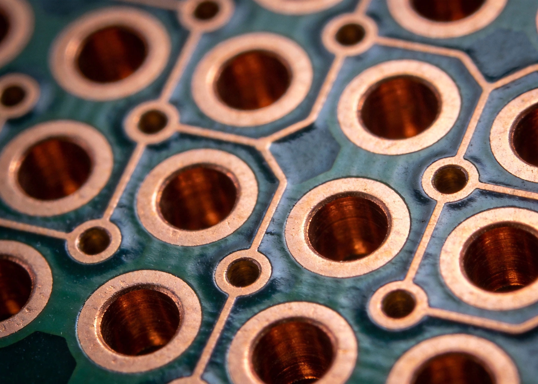
To understand why microvia testing demands special attention, it helps to understand what makes microvias fundamentally different from the through-hole vias that dominated Pcb Manufacturing for decades.
Standard through-hole vias connect the top layer to the bottom layer of a PCB and are drilled after the board is fully laminated. Their diameters range from 0.2 millimeters to 1.0 millimeters or more, and their length is the full thickness of the board. Microvias, by contrast, are typically laser-drilled and connect only adjacent layers—layer 1 to layer 2, or layer 2 to layer 3—rather than spanning the entire board depth. They are formed before the final lamination step, often within a sub-assembly, which means the plating solution must fill a relatively short but narrow hole without the benefit of through-flow that assists plating in through-holes.
The aspect ratio of a microvia—the ratio of its depth to its diameter—is typically much lower than that of a through-hole, often between 0.5:1 and 1:1, which sounds like it should make plating easier. In practice, the small diameter of the microvia opening creates surface tension challenges for solder paste application and can trap air bubbles during plating. Additionally, microvias are frequently used in stacked configurations where one microvia is placed directly on top of another to create a conductive path through multiple layers. If either microvia in the stack fails, the entire chain is broken. The reliability of stacked microvia structures is only as strong as the weakest link in the chain.
Microvia failures do not happen randomly. They follow predictable patterns that are tied to specific manufacturing defects, design choices, or stress conditions during the board's operational life. Understanding these failure mechanisms is the first step toward designing tests that catch them.
The most common manufacturing defect in microvias is void formation during the Copper Plating process. A void is a small pocket of air or gas trapped inside the plated microvia barrel. Even a small void—covering 10 to 15 percent of the cross-sectional area—significantly weakens the microvia mechanically and creates a stress concentration point where cracking initiates under thermal cycling. Larger voids can create an open circuit immediately after plating, causing the board to fail even before it reaches assembly.
Voids form when air bubbles are trapped inside the microvia cavity during the plating solution fill process, when organic contamination on the via wall prevents copper from depositing uniformly, or when the plating current profile is not optimized for the specific geometry of the microvia. Achieving void-free microvia plating requires precise control of plating chemistry, adequate solution agitation, and often pulse-reverse plating techniques that help solution penetrate the microvia cavity and clear trapped gas.
Even a perfectly plated, void-free microvia can fail in the field under repeated thermal cycling. When a PCB powers on, the components generate heat, which raises the board temperature. When the device powers off, it cools. This thermal cycling causes the copper inside the microvia and the surrounding Dielectric Material to expand and contract at different rates, creating cyclic stress on the copper barrel. Over thousands of cycles, this stress can cause the copper to crack—a phenomenon called thermal fatigue failure.
The risk of thermal fatigue is higher in microvias than in through-hole vias for two reasons. First, the copper barrel in a microvia is relatively short and constrained, which concentrates stress at the interface between the microvia barrel and the landing pad. Second, Hdi Boards are frequently used in applications with wide temperature ranges—automotive under-hood electronics, outdoor industrial equipment, aerospace systems—all of which experience aggressive thermal cycling. Boards that pass initial electrical testing can develop microvia cracks after months or years of thermal cycling in the field, which is why some testing standards require accelerated thermal cycling as part of the qualification process.
Electromigration is a gradual failure mechanism where copper atoms physically migrate through the Dielectric Material under the influence of sustained high current density. In microvias carrying current between power planes, the current density can be very high because the cross-sectional area of the microvia barrel is tiny. Over time, copper atoms migrate away from the high-current-density areas, creating voids that eventually open the circuit. Electromigration failures typically occur after extended operation—hundreds or thousands of hours—and are therefore difficult to catch in standard production testing, which is why design rules that limit current density in microvias are so important.
The interface between the microvia barrel and the landing pad on adjacent layers is a mechanically vulnerable region. If the copper-to-dielectric adhesion at this interface is weak, thermal cycling can cause the pad to separate from the underlying dielectric—a phenomenon sometimes called Pad Cratering. This creates an intermittent or permanent open circuit that is difficult to diagnose because the defect may only manifest under specific thermal conditions. Delamination risk is higher when the microvia is located over a plane split or a large reference plane void, which creates uneven thermal stress distribution.
Design and manufacturing alignment issues compound microvia reliability challenges. If a microvia is drilled slightly off-center from its landing pad, the copper barrel may be thinner on one side, creating a mechanical weak point. This registration error is more consequential for microvias than for standard through-hole vias because the pads are smaller and the tolerance budget is tighter. Similarly, if the land diameter—the pad at the bottom of the microvia—is too small relative to the drill diameter, the plating has less area to bond to, which increases the risk of interfacial failure.
Traditional Pcb electrical testing methods were developed for through-hole vias and are often inadequate for detecting the subtle defects that cause microvia field failures.
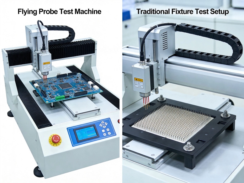
Flying probe testing, which uses spring-loaded pins to make temporary electrical contact with board test points, works by driving current through a net and measuring resistance. For a through-hole via that is completely open, flying probe will detect the failure instantly. But a microvia with a 30 percent void that has not yet cracked will test as a good connection at room temperature because the remaining copper cross-section is still sufficient to carry the low test current. The defect only manifests under thermal stress, when the cracked or voided copper separates further. Standard flying probe testing at room temperature simply cannot detect this class of latent defect.
Continuity testing with low current levels is similarly insufficient. Many microvia reliability failures are current-density-dependent or thermal-cycle-dependent, and a test that applies milliamps of current at room temperature provides no information about how the microvia will behave under operational conditions. This is why additional testing methods are essential for Hdi Boards destined for demanding applications.
Testing microvia resistance under high current conditions simulates the electromigration and thermal stress that microvias experience in actual operation. By driving current levels closer to operational current densities through the microvia and monitoring resistance over time, this test can identify microvias that are vulnerable to electromigration failure or that show resistance drift indicative of emerging thermal fatigue cracks. High-current testing is particularly important for power delivery microvias in HDI boards where current density per via can be surprisingly high due to the small barrel diameter.
Accelerated life testing through temperature cycling exposes boards to repeated thermal transitions between hot and cold temperature extremes. A typical thermal cycling test might cycle between minus 40 degrees Celsius and plus 125 degrees Celsius for 500 to 1,000 cycles, which simulates months or years of operational thermal stress in a compressed timeframe. Electrical testing performed before, during, and after thermal cycling reveals microvias that develop opens or increased resistance under thermal stress. Any board that shows resistance change greater than the specified threshold after thermal cycling should be rejected.
Temperature cycling is expensive and time-consuming and is typically reserved for qualification testing of new designs rather than production testing of every board. However, for military, aerospace, and medical applications where microvia reliability is non-negotiable, temperature cycling is effectively mandatory as part of the qualification process.
Isolation resistance testing measures the resistance between adjacent nets to detect any leakage current that might indicate insulation breakdown. In microvia密集的 HDI boards with tightly spaced traces and microvias, insulation resistance between adjacent circuits is a critical quality parameter. Contamination inside or near a microvia, or dielectric breakdown between a microvia barrel and an adjacent trace, creates a leakage path that isolation resistance testing can detect. This test is particularly valuable for high-voltage applications where the risk of dielectric breakdown is elevated.
Time Domain Reflectometry (Tdr) testing sends a fast pulse through a trace or microvia and analyzes the reflected signal to characterize impedance and detect discontinuities. A microvia that has a different impedance than the trace it connects to causes a reflection that Tdr can detect even when the microvia appears to have normal DC continuity. Impedance discontinuities in high-speed signal paths can cause signal reflection, ringing, and data errors at gigabit-per-second data rates. TDR testing is an essential tool for validating high-speed HDI designs where microvia stubs and impedance mismatches degrade Signal Integrity.
After boards go through the solder reflow process, the thermal stress of the reflow cycle can cause microvias that were marginally manufactured to fail. Measuring microvia resistance before and after a simulated reflow profile—a process sometimes called solder float testing or thermal stress testing—exposes these marginal defects. The board is floated in molten solder at 260 to 288 degrees Celsius for a defined duration, and resistance is measured immediately afterward and after a recovery period. Any significant resistance increase after solder float indicates a microvia that is too weak to survive the assembly process.
While testing is essential for verifying microvia quality, the most reliable microvias are those that are designed and manufactured correctly from the start. Design for Manufacturability (DFM) practices play a crucial role in ensuring microvia reliability that no amount of testing can fully substitute for.
Stacked microvia configurations—where one microvia lands on top of another—should be used conservatively. Each additional layer in a microvia stack adds another potential failure point. A two-layer microvia stack is generally reliable if both microvias are manufactured to good quality standards. Stacking three or more microvias in sequence requires exceptional process control and is typically reserved for the most demanding applications where the routing density benefit justifies the reliability risk.
The choice of microvia land sizes and capture pad diameters affects both manufacturing yield and long-term reliability. Oversizing the capture pad—the pad that the microvia lands on—provides more plating area and a more robust mechanical bond. Many designers use capture pad diameters that are 0.15 to 0.2 millimeters larger than the microvia drill diameter, which dramatically improves reliability at minimal routing cost. This oversizing is particularly valuable for the bottom microvia in a stack, where stress concentration is highest.
Via-in-pad configurations—where a microvia is placed directly in the center of a component pad rather than offset to the side—are popular for space-constrained designs but require special manufacturing attention. The thermal relief from the plane connections around a Via-in-pad must be carefully designed to balance solder capture with Thermal Performance, and the plating quality inside the microvia must be exceptional because there is no margin for marginal adhesion.
Several industry standards govern microvia reliability testing and provide acceptance criteria for different application classes. Understanding these standards helps designers specify the right testing requirements for their applications.
IPC-2226, the standard for Hdi Pcb design, defines microvia geometry and performance classes. IPC-4104 defines material requirements for HDI boards. For microvia reliability testing, IPC-T-50 and IPC-6018 provide test methods and acceptance criteria for microvia thermal cycling, resistance measurement, and insulation resistance. MIL-PRF-31032 and MIL-PRF-55110 provide military-specific requirements for boards used in defense applications, with more stringent thermal cycling and electrical testing requirements than commercial standards.
For Medical Electronics, IEC 60601 and the associated board-level standards impose additional reliability and traceability requirements that extend beyond standard commercial testing. Automotive Electronics must meet Aec-q100 and AEC-Q200 qualification requirements, which include specific temperature cycling and electrical testing protocols for boards used in automotive environments.
A microvia is a small-diameter via, typically 0.15 millimeters or less, that connects adjacent layers and is almost always laser-drilled. A Buried Via is a via that is formed inside the board and is not visible on the outer surfaces—it may be a standard through-hole or a larger-scale via that has been buried during a Sequential Lamination process. The two terms describe different characteristics: microvia describes the via's size and drilling method, while buried describes its position relative to the outer surfaces. A buried microvia combines both attributes—a small, laser-drilled via that connects internal layers without reaching the board surface.
Microvia void content is most reliably measured through cross-sectional analysis, where a sample microvia is cut, mounted in epoxy, polished to a mirror finish, and examined under a microscope. The percentage of the microvia cross-sectional area that is voided—rather than filled with copper—is calculated as the void content. X-ray Inspection using computed tomography (CT scan) can provide three-dimensional void visualization non-destructively, but this equipment is expensive and not available at all manufacturing facilities. Some manufacturers use acoustic microscopy or scanning acoustic tomography as a non-destructive screening tool, though cross-sectioning remains the definitive method.
Standard flying probe testing can detect a microvia that is completely open, but it typically cannot detect latent defects such as partial voids, minor plating thinning, or micro-cracks that have not yet propagated to full open conditions. These latent defects only manifest under thermal cycling or high-current stress. For HDI boards used in high-reliability applications, flying probe testing should be supplemented with thermal cycling tests, solder float tests, or high-current stress tests that stress the microvia in ways that reveal marginal quality.
The required number of thermal cycles depends on the application. Commercial electronics typically need to survive 100 to 300 temperature cycles without failure. Automotive Electronics under Aec-q100 requirements face more demanding conditions and typically require 1,000 or more cycles. Military and aerospace boards may need to survive 2,000 to 3,000 cycles depending on the specific environmental requirements. The test temperature range also matters—a board tested between minus 40 and plus 85 degrees Celsius faces less stress than one tested between minus 55 and plus 125 degrees Celsius.
At minimum, every production HDI board should receive continuity testing to verify that all nets are electrically connected, isolation resistance testing to verify that no adjacent nets are shorted, and solder float or simulated reflow stress testing to verify that microvias survive the assembly thermal cycle. For boards used in high-reliability applications, additional thermal cycling, high-current stress testing, and TDR impedance characterization should be added. The exact test plan should be defined by the application reliability requirements and specified in the procurement documentation.
Microvia reliability is not a concern that can be addressed after the design is complete—it must be considered at every stage, from the initial stack-up and via strategy decisions through manufacturing process control to the final electrical test report. The failure mechanisms that threaten microvia integrity—void formation, thermal fatigue, electromigration, and delamination—are subtle, sometimes latent, and can cause field failures that are extremely costly in terms of warranty cost, reputational damage, and in safety-critical applications, potential harm to users.
The good news is that microvia reliability is highly manageable when approached systematically. Designing with adequate capture pad sizes, using conservative stacked microvia strategies, selecting the right materials and plating processes, and specifying appropriate electrical testing all contribute to a reliable end product. No single step is sufficient on its own, but the combination of good design, rigorous process control, and comprehensive testing creates a defense-in-depth strategy that catches defects at multiple stages and minimizes the probability of field failures.
For engineers specifying HDI boards and for quality teams defining test protocols, the message is clear: investing in thorough microvia electrical testing is not an expense—it is insurance against the far greater cost of field failures. When the alternative is a device failure in the hands of a customer, a medical patient, or a passenger in an aircraft, the cost of comprehensive microvia testing looks modest by comparison.
This article is provided for general informational purposes regarding microvia reliability and electrical testing methods for HDI PCBs. Specific testing requirements and acceptance criteria should be determined based on your application's reliability requirements and applicable industry standards. Consult with your PCB manufacturer and quality engineering team for design-specific guidance.

Mastering Stack-up Design for Optimal HDI PerformanceJune/08/2026
Non-Destructive Testing Techniques for Multilayer HDI PCBsSeptember/29/2026

Overcoming the Challenges of Testing Fine-Pitch BGA on HDISeptember/04/2026
Designing for Manufacturing (DFM): Avoiding Common HDI PitfallsSeptember/02/2026
Advanced Testing Methods for High-Density Interconnect PCBsMay/28/2026
How X-Ray Inspection (AXI) Detects Hidden Defects in HDI BoardsJuly/30/2026
Best Practices for BGA Fanout and Routing in HDI LayoutsJuly/07/2026
Flying Probe vs. Fixture Testing: Which is Best for HDI PCBs?June/11/2026