
Ever had a board that looked perfect on screen but failed EMC testing the first time? Yeah, me too. It’s honestly the worst feeling. The problem usually isn't your routing, it's the foundation. Mastering stack-up design for optimal HDI performance is way more than just stacking layers on top of each other. It’s about building a solid electrical home for your signals. Here, we’ll dig into real strategies, mistakes I’ve made so you don’t have to, and how to actually get it right.
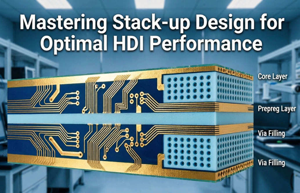
HDI tech is great, smaller vias, tighter lines, more room. But it’s also a minefield. When you're mastering stack-up design for optimal HDI performance, you gotta juggle Signal Integrity, power noise, and heat all at once. A bad stack-up? That’s a one-way ticket to crosstalk and impedance nightmares. I once saw a PCIe bus fail just because a prepreg was off by a few mils. Crazy, right? Shows how sensitive this stuff is.
Also, think about return paths. Microvias and Blind Vias are cool, but if your reference plane is split or too far, the signal’s gonna leak noise everywhere. Every layer needs a job. Don't just add layers because you can't route; plan them to actually support the electronics.
Symmetry is key, seriously. Asymmetrical stack-ups warp during reflow. Warped boards mean assembly headaches and reliability issues down the road. Try to balance copper and dielectric thickness around the center core. It’s not always easy, but it’s worth it.
Another big one: keep signal layers next to solid planes. High-speed signals need a return path right underneath. If you route over a split power plane, the return current jumps the gap and boom, you got an antenna. I see this mistake a lot. Dedicate layers for ground and power, keep them tight. Closer planes mean better decoupling capacitance, which helps kill power noise.
Materials matter more than people think. Standard FR4 is fine for slow stuff, but HDI? You probably need low-loss. When mastering stack-up design for optimal HDI performance, check the Dk And Df. Stable Dk means consistent impedance. If Dk varies across the panel, you’ll miss your targets. Simple as that.
Thermal stuff too. Hdi Boards go through multiple laminations. If materials have mismatched CTE, you get reliability issues. Talk to your fab house early. They know what works. And hey, expensive isn't always better. Sometimes a hybrid stack-up with standard FR4 inside and low-loss outside is the sweet spot for cost and performance.
Vias are bridges, but they’re also parasites. Microvias help escape BGAs, but stubs cause reflections at high speeds. When mastering stack-up design for optimal HDI performance, handle those stubs. Back-drill or use Blind Vias that don't go all the way through. It helps.
Spacing matters too. Don't pack vias too close, or you get crosstalk. Rule of thumb: keep them 3x drill diameter apart. And put ground vias near signal vias when changing layers. It gives the return current a path. Simple fix, huge difference for EMI.
Biggest mistake? Ignoring what the fab can actually build. Designing a stack-up that’s impossible to manufacture is just wasting time. Check aspect ratios. Thick board plus tiny microvias? Plating might fail. Also, don't forget solder mask. In HDI, it actually affects impedance. Include it in your calcs.
And simulation. Hand calcs are okay, but field solvers are better. When mastering stack-up design for optimal HDI performance, verify impedance and crosstalk before you send it out. Adds a few days now, saves weeks of debugging later. Trust me.
Wrapping It Up
So yeah, mastering stack-up design for optimal HDI performance is a balancing act. Electromagnetics, materials, manufacturing, cost. But if you stick to symmetry, keep solid reference planes, and pick materials wisely, you’ll build boards that actually work.
Take a look at your current stack-ups. Got enough margin for tolerances? Simulated the critical nets? Try these tips on your next project. You’ll see the difference. Got questions or war stories? Drop a comment below.
Q: How many layers for HDI?
A: Depends on density. Usually starts at 6, but complex stuff hits 12+. Focus on routing density, not just layer count.
Q: Can I use standard FR4?
A: For slow signals, sure. High-speed serial? Get low-loss to save your Insertion Loss.
Q: Most important stack-up rule?
A: Every high-speed signal layer needs an adjacent solid reference plane. Non-negotiable.
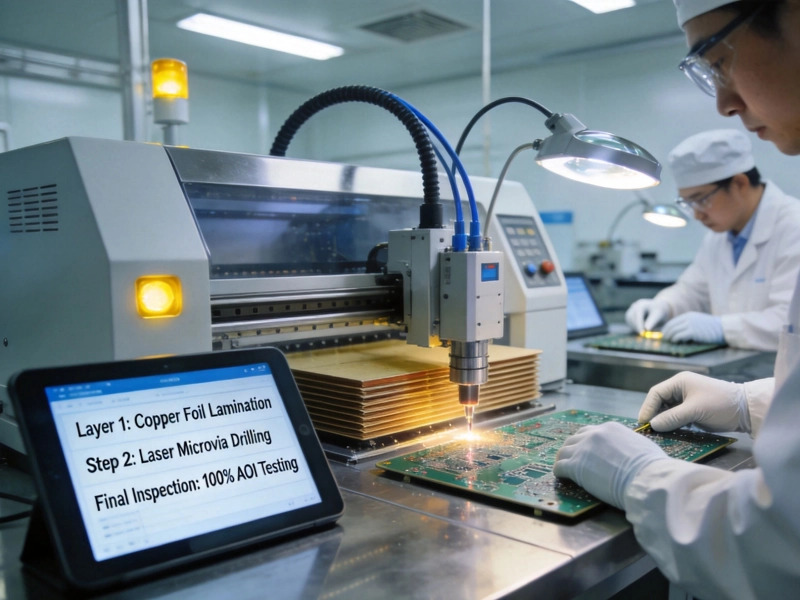
A Step-by-Step Walkthrough of the HDI PCB Manufacturing ProcessMay/28/2026
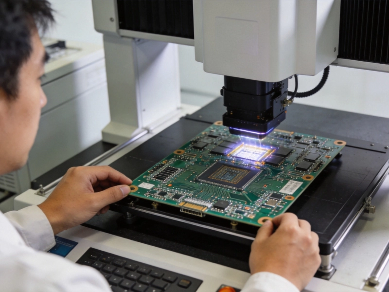
Non-Destructive Testing Techniques for Multilayer HDI PCBsSeptember/29/2026
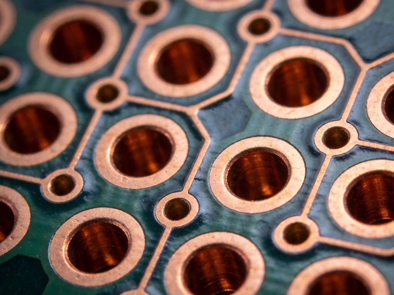
The Importance of Electrical Testing for Microvia ReliabilityJuly/09/2026
How X-Ray Inspection (AXI) Detects Hidden Defects in HDI BoardsJuly/30/2026
The Art of Microvia Placement: Staggered vs. Stacked ViasSeptember/24/2026
Designing for Manufacturing (DFM): Avoiding Common HDI PitfallsSeptember/02/2026
Best Practices for BGA Fanout and Routing in HDI LayoutsJuly/07/2026
Designing HDI Backplanes for High-Performance Networking EquipmentOctober/16/2026