Open Nav

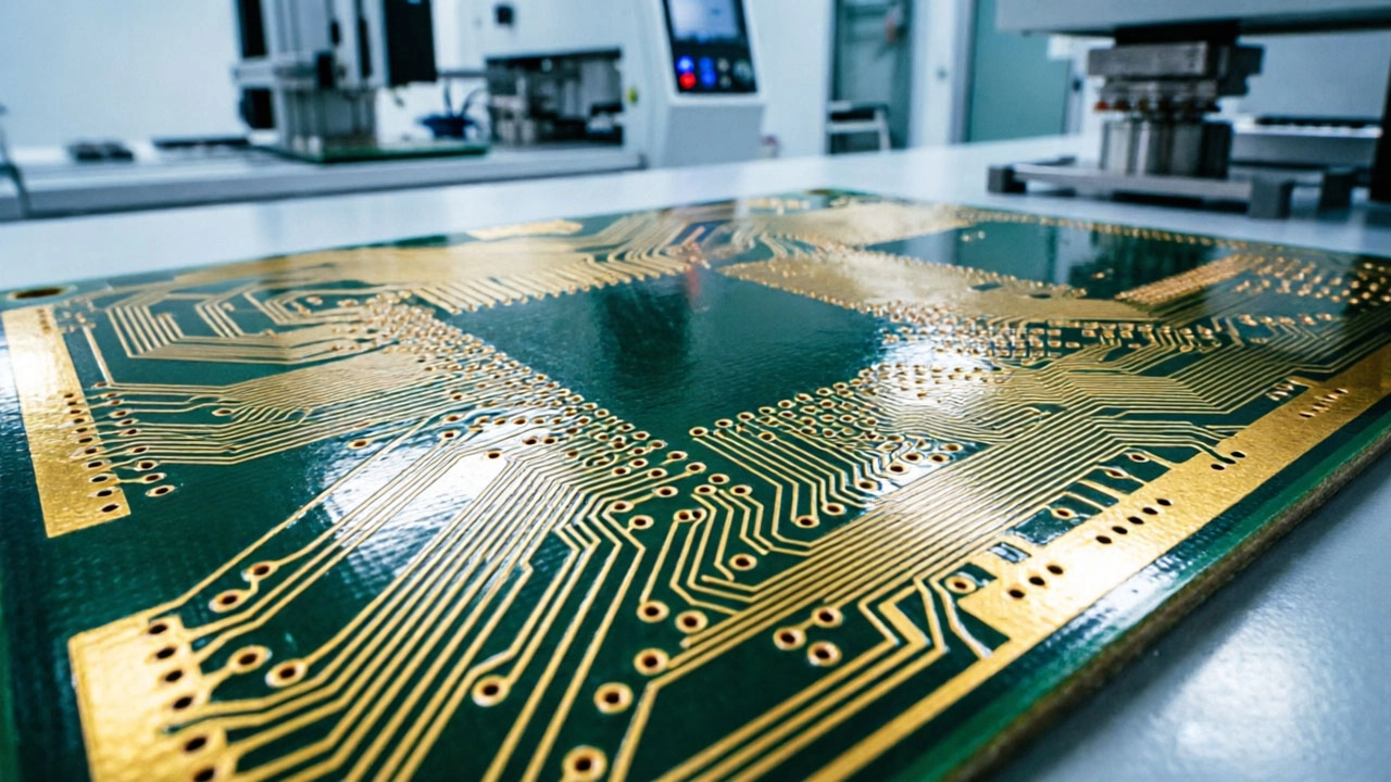
High-Density Interconnect (HDI) technology has revolutionized modern electronics, allowing for smaller form factors and higher functionality in devices ranging from smartphones to aerospace avionics. However, as trace widths shrink and signal frequ...
https://www.high-density-interconnect-pcb.comhttps://www.high-density-interconnect-pcb.com/hdi-pcb-materials/selecting-the-right-dielectric-materials-for-high-performance-hdi-pcbs-43/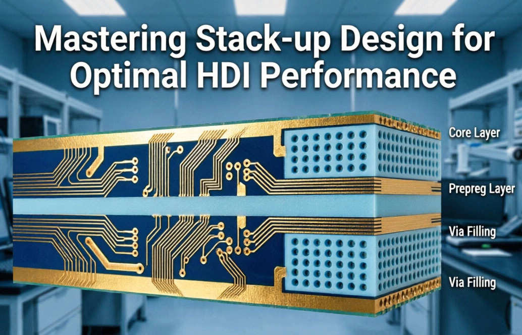
Ever had a board that looked perfect on screen but failed EMC testing the first time? Yeah, me too. It’s honestly the worst feeling. The problem usually isn't your routing, it's the foundation. Mastering stack-up design for optimal HDI performance ...
https://www.high-density-interconnect-pcb.comhttps://www.high-density-interconnect-pcb.com/hdi-pcb-design-testing/mastering-stack-up-design-for-optimal-hdi-performance/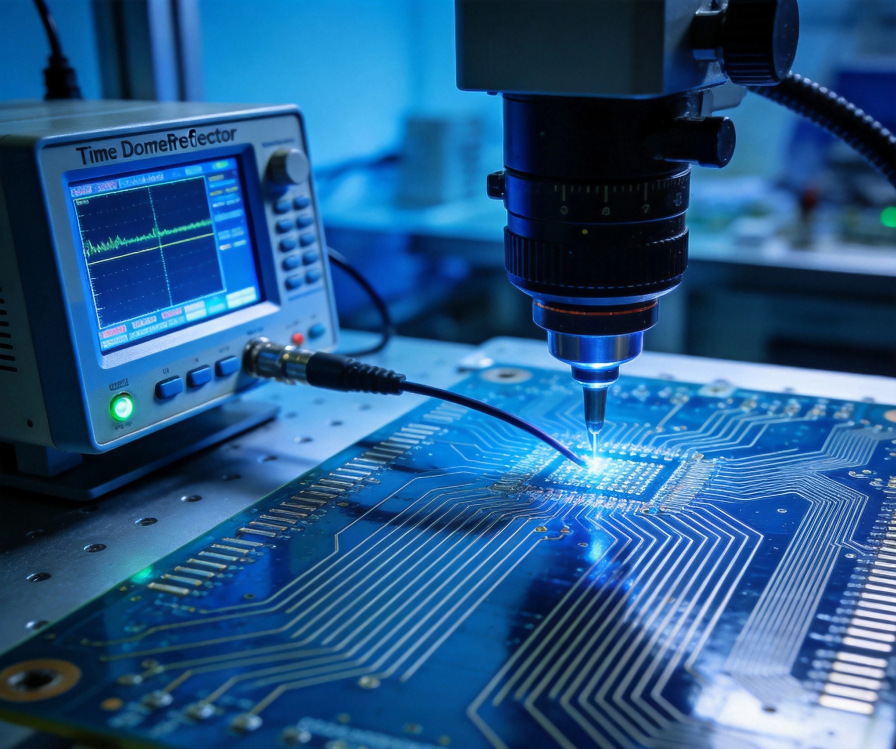
High density interconnect (HDI) boards enable the miniaturization and performance requirements of modern electronics, but these benefits come with increased complexity in impedance control. As trace widths decrease, layer counts increase, and featu...
https://www.high-density-interconnect-pcb.comhttps://www.high-density-interconnect-pcb.com/hdi-pcb-faq-support/how-to-measure-and-control-impedance-tolerance-in-hdi-boards/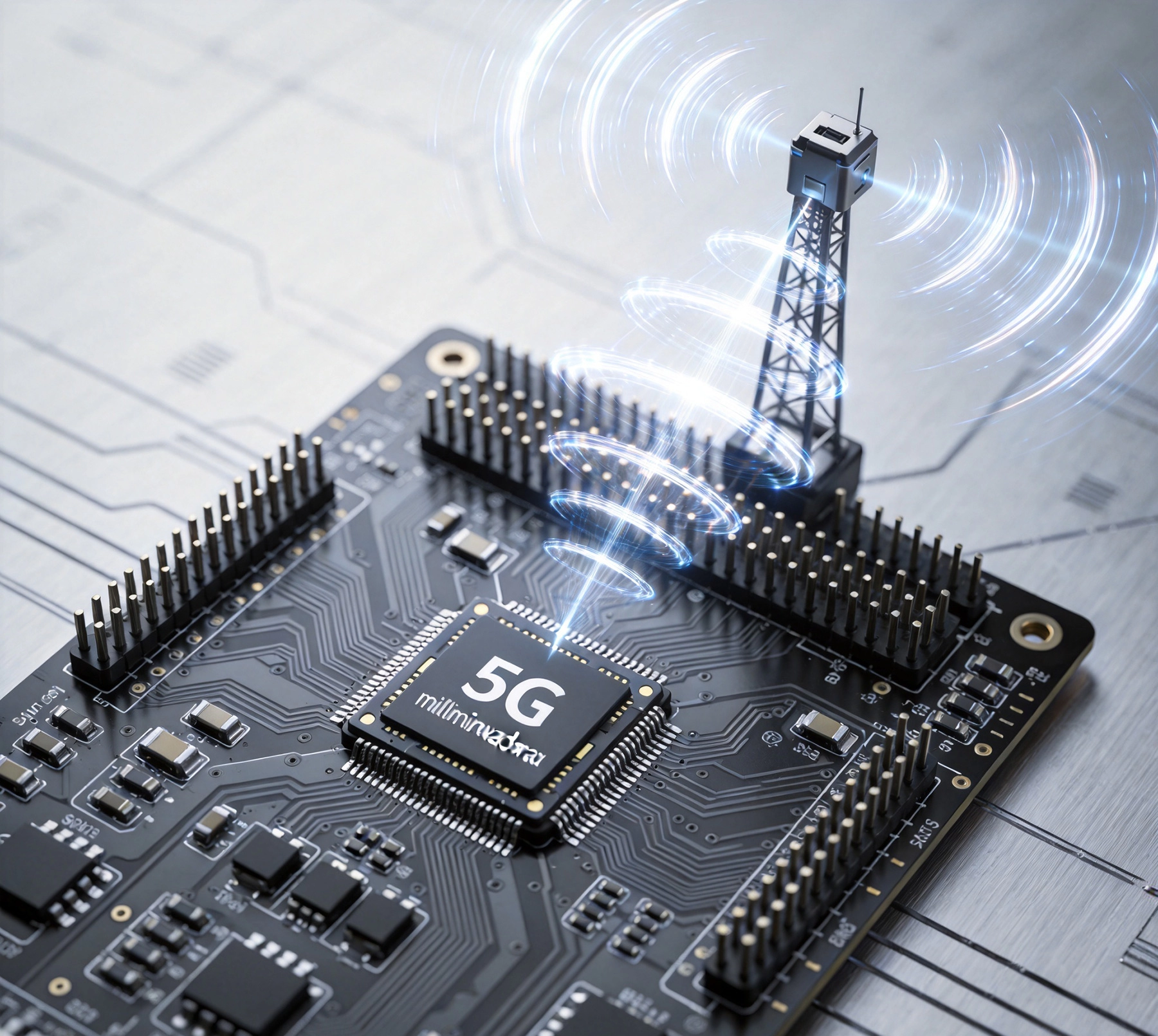
The transition to 5G millimeter wave frequencies presents PCB designers with challenges that dwarf those encountered at traditional microwave frequencies. While sub-6GHz cellular infrastructure shares many characteristics with established RF design...
https://www.high-density-interconnect-pcb.comhttps://www.high-density-interconnect-pcb.com/telecom-5g-high-speed-computing/signal-integrity-challenges-in-5g-mmwave-hdi-designs/