
Misinterpreting HDI stack-up drawings causes manufacturing failures, design rejections, and expensive rework cycles.
High-density Interconnect (HDI) PCBs have become essential for modern electronics, enabling smaller form factors and higher functionality. But these advanced boards require sophisticated stack-up designs that go far beyond traditional multilayer PCBs. Reading and interpreting HDI stack-up drawings correctly is critical for successful manufacturing, cost control, and performance optimization.
This comprehensive guide breaks down HDI stack-up drawings into understandable components, explaining what each element means and how to interpret design specifications correctly.
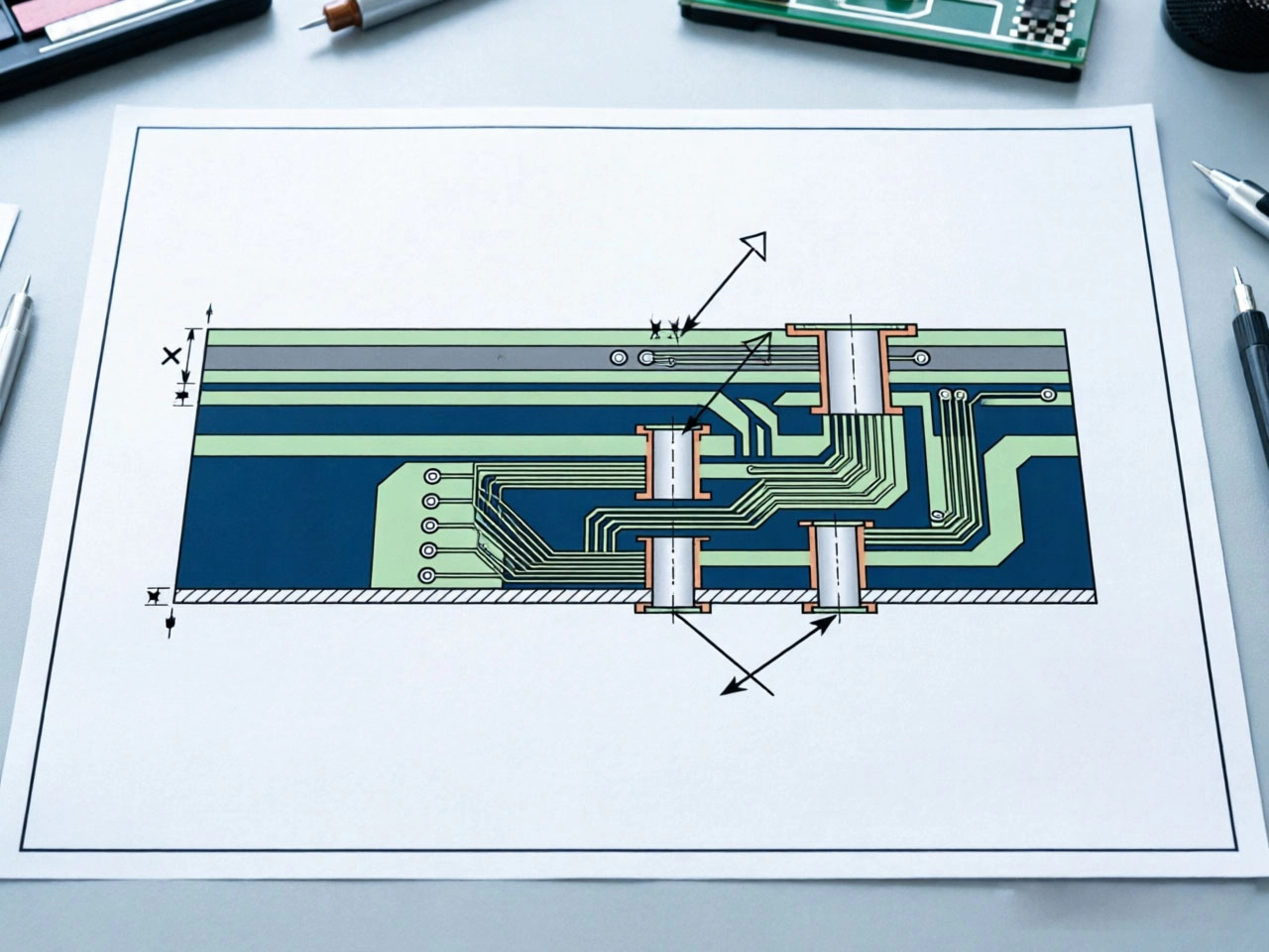
Before diving into stack-up drawings, it's essential to understand what makes HDI PCBs unique:
Stack-up drawings are the blueprints that define: - Layer order and materials - Copper thickness for each layer - Via connections between layers - Electrical characteristics (impedance, power distribution) - Manufacturing requirements and constraints
Misinterpreting these drawings leads to boards that don't work, won't manufacture properly, or fail reliability testing.
HDI stack-up drawings contain multiple sections, each conveying critical information:
The layer overview shows the overall board structure: - Total layer count (typically 8-20+ layers for HDI) - Layer numbering sequence (Top layer to bottom layer) - Signal, power, and ground plane assignments - Material stack-up (core materials and prepreg thicknesses)
Reading tip: Start here to understand the overall structure before diving into details. The layer sequence determines routing density and complexity.
Each copper layer has detailed specifications: - Copper weight: Typically 0.5oz-2oz for HDI (18μm-70μm) - Layer type: Signal, power plane, ground plane, or mixed - Electrical characteristics: Impedance requirements, current capacity - Surface finish: Plating,HASL, ENIG, or other finishes
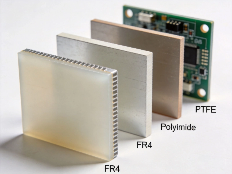
Dielectric layers between copper define electrical properties: - Material type: FR4, high-Tg FR4, polyimide, or advanced laminates - Thickness: Typically 0.1mm-0.2mm for HDI - Dielectric constant (Dk): 3.5-4.5 for FR4, lower for advanced materials - Dielectric Loss (Df): 0.015-0.025 for standard FR4
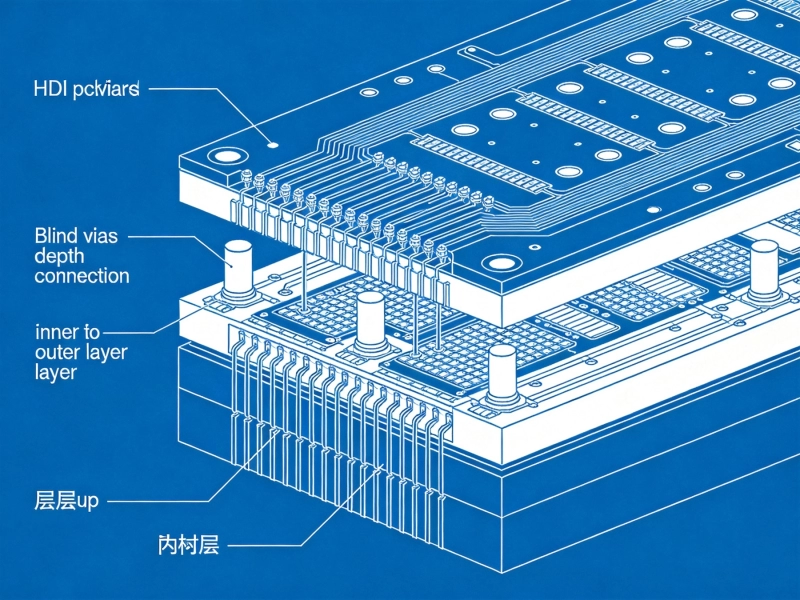
HDI vias come in several types, each clearly specified: - Through vias: Pass through entire board (traditional) - Blind Vias: Connect outer layers to inner layers only - Buried Vias: Connect inner layers without reaching surfaces - Micro Vias: Laser-drilled small-diameter vias (0.1-0.15mm)
Controlled impedance requirements include: - Target impedance: Typically 50Ω, 100Ω differential, or other values - Trace width and spacing: Dimensional requirements for Impedance Control - Dielectric thickness: Stack-up adjustments to achieve target impedance - Tolerance requirements: Typically ±10% for controlled impedance
Let's examine how to interpret specific layer configurations:
Outer layers typically include: - Signal routing: Most routing occurs on outer layers for accessibility - Component placement: Components mounted on outer layers - Surface finish: Specified as HASL, ENIG, OSP, or other - Copper weight: Often 1oz or 2oz for durability
Inner signal layers provide additional routing capacity: - Routing direction: Often alternating (horizontal vs. vertical) between layers - Impedance Control: Critical for high-speed signals - Copper weight: Typically 0.5oz or 1oz for space efficiency- Reference planes: Each signal layer should have adjacent reference plane
Power distribution planes serve critical functions: - Ground planes: Provide return paths for signals and shielding - Power planes: Distribute power voltage throughout the board - Split planes: Multiple voltage levels separated in same plane - Plane connections: Via connections for power distribution
HDI via structures are more complex than traditional through vias:
Micro vias are HDI's defining characteristic: - Diameter: 0.1-0.15mm typical - Aspect ratio: Typically 0.8:1 (depth to diameter) - Drilling method: Laser Drilling (CO2 or UV laser) - Connection depth: Typically 1-3 layers deep
Blind Vias connect outer layers to specific inner layers: - Layer 1-2 vias: Connect top layer to layer 2 - Layer 1-3 vias: Connect top layer to layer 3 - Sequential connections: Multiple blind vias stacked to reach inner layers - Relay connections: Use multiple short vias instead of one deep via
Buried vias connect inner layers only: - Layer 2-3 vias: Connect layers 2 and 3 - Layer 4-5 vias: Connect layers 4 and 5 - Complex routing: Enable routing density increases - Sequential Lamination: Required for multiple Buried Via levels
Advanced HDI uses vias directly in component pads: - Space savings: Eliminates via space outside component pads - Routing efficiency: Enables higher component density - Manufacturing challenges: Requires special processes - Thermal benefits: Improves heat transfer from components
Stack-up drawings specify critical tolerances:
Dielectric thickness variations affect electrical performance: - Core thickness tolerance: Typically ±10% - Prepreg thickness tolerance: ±10-15% - Copper thickness tolerance: ±10% for outer layers, ±15% for inner - Total board thickness: ±10% tolerance typical
Via dimensions have tight tolerances for reliability: - Micro via diameter: ±0.02mm - Via plating thickness: Minimum 20μm - Via capture pad size: Specified minimum and maximum - Via-to-feature spacing: Minimum spacing requirements
Trace and space dimensions define manufacturability: - Minimum trace width: Specified absolute minimum - Minimum trace spacing: Critical for Signal Integrity - Trace width tolerance: ±20% typical - Copper edge tolerance: ±0.1mm for outer features
Stack-up drawings specify material requirements:
Stack-up drawings define electrical requirements:
Stack-up drawings include manufacturing requirements:
Understanding common configurations helps in interpretation:
One build-up cycle on each side: - Structure: Top build-up + core + bottom build-up - Vias: Blind vias on outer layers, through vias in core - Applications: Moderate complexity Hdi Boards
Two build-up cycles on each side: - Structure: 2-layer build-up + core + 2-layer build-up - Vias: Two levels of blind vias on each side - Applications: High-density routing requirements
Vias can connect any adjacent layer combination: - Structure: Multiple build-up layers on each side - Vias: Micro vias connect any adjacent layer pair - Applications: Highest density and flexibility
Let's interpret a typical HDI stack-up:
Layer structure (top to bottom): 1. Layer 1 (top): Signal, 1oz copper, ENIG finish 2. Layer 2: Signal, 0.5oz copper, referenced to layer 3 3. Layer 3: Ground plane, 1oz copper 4. Layer 4: Signal, 0.5oz copper, referenced to layer 5 5. Layer 5: Power plane, 1oz copper 6. Layer 6: Power plane, 1oz copper 7. Layer 7: Signal, 0.5oz copper, referenced to layer 6 8. Layer 8: Ground plane, 1oz copper 9. Layer 9: Signal, 0.5oz copper, referenced to layer 8 10. Layer 10 (bottom): Signal, 1oz copper, ENIG finish
Via structure: - Blind vias: Layers 1-2 and 9-10 (laser micro vias, 0.1mm diameter) - Through vias: Connect all layers - Buried vias: Layers 2-3, 4-5, 6-7, 7-8
Dielectric thickness: - Core thickness: 0.8mm - Build-up dielectric: 0.1mm each layer - Total board thickness: 1.2mm
Common error: Assuming blind vias connect to all layers. Correction: Blind vias connect only specified layers. Check stack-up drawing carefully for exact layer connections.
Common error: Ignoring dielectric thickness variations on impedance. Correction: Dielectric thickness tolerance affects impedance significantly. Calculate impedance range based on thickness variations.
Common error: Assuming single lamination for all layers. Correction: Multiple build-up layers require sequential lamination. Each lamination cycle adds cost and affects manufacturability.
Common error: Assuming unlimited via stacking is possible. Correction: Via stacking has limitations based on aspect ratio and reliability requirements. Consult manufacturer capabilities.
Reading and interpreting Hdi Pcb stack-up drawings correctly is essential for successful high-density Electronics Design. These drawings contain the complete specification for manufacturing complex multilayer boards with advanced via structures and tight tolerances.
Understanding layer configurations, via structures, material specifications, and manufacturing requirements enables designers to create Hdi Boards that meet performance, cost, and manufacturability goals. The investment in learning to read these drawings properly prevents costly manufacturing failures and design rejections.
As electronics continue pushing density limits, Hdi Technology becomes increasingly important. Mastery of stack-up drawing interpretation provides the foundation for leveraging HDI capabilities in your designs.
Need help with your Hdi Pcb Stack-up Design? Work with experienced PCB manufacturers who understand HDI requirements. Their expertise in material selection, via design, and manufacturing processes ensures your HDI boards achieve your design goals while maintaining manufacturability and cost-effectiveness.
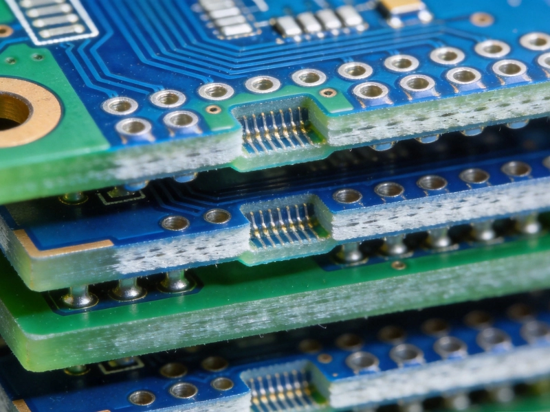
An Introduction to Microvia Technology in HDI PCBsJuly/24/2026
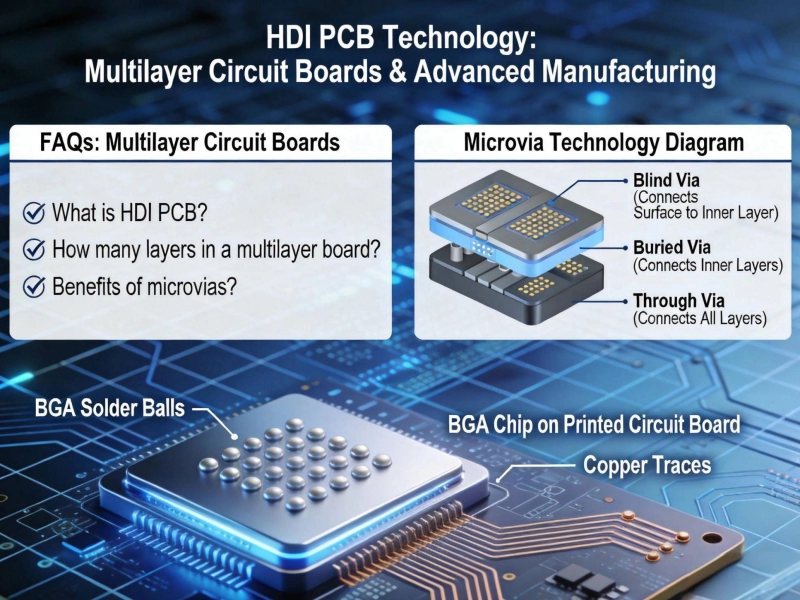
Top 10 Frequently Asked Questions About HDI PCB TechnologyMay/28/2026

Implementing a Robust Quality Control System for HDI ManufacturingJune/15/2026
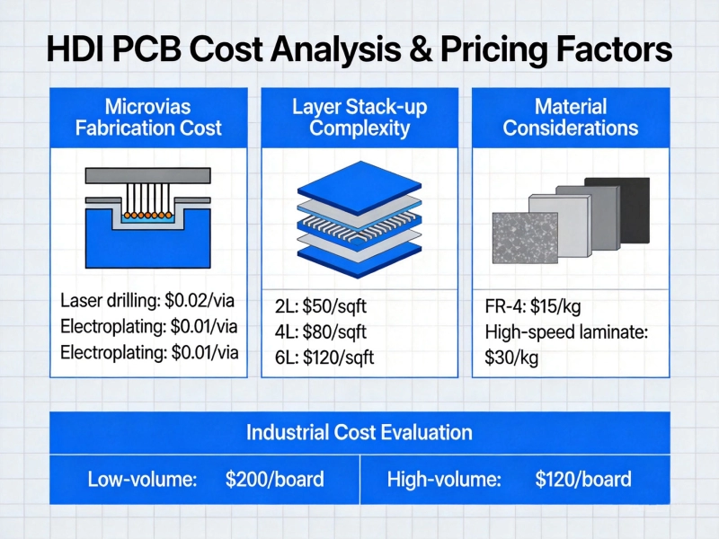
HDI PCB Cost Guide: What Factors Drive the Price Up?June/16/2026
Understanding HDI Terminology: A Glossary for EngineersAugust/03/2026
Troubleshooting Common Issues in HDI PCB AssemblySeptember/09/2026

How to Measure and Control Impedance Tolerance in HDI BoardsAugust/03/2026
Selecting the Right Dielectric Materials for High-Performance HDI PCBsMay/28/2026