
Beyond documentation, dedicated engineering support plays a crucial role in the success of a High Density Interconnect PCB project. Expert teams assist with Design for Manufacturability (DFM) reviews, stack-up optimization, and material selection to ensure the final product meets strict electrical and reliability standards. This collaborative approach bridges the gap between innovative design and practical fabrication, ensuring a smooth transition from prototype to mass production for advanced electronic devices.
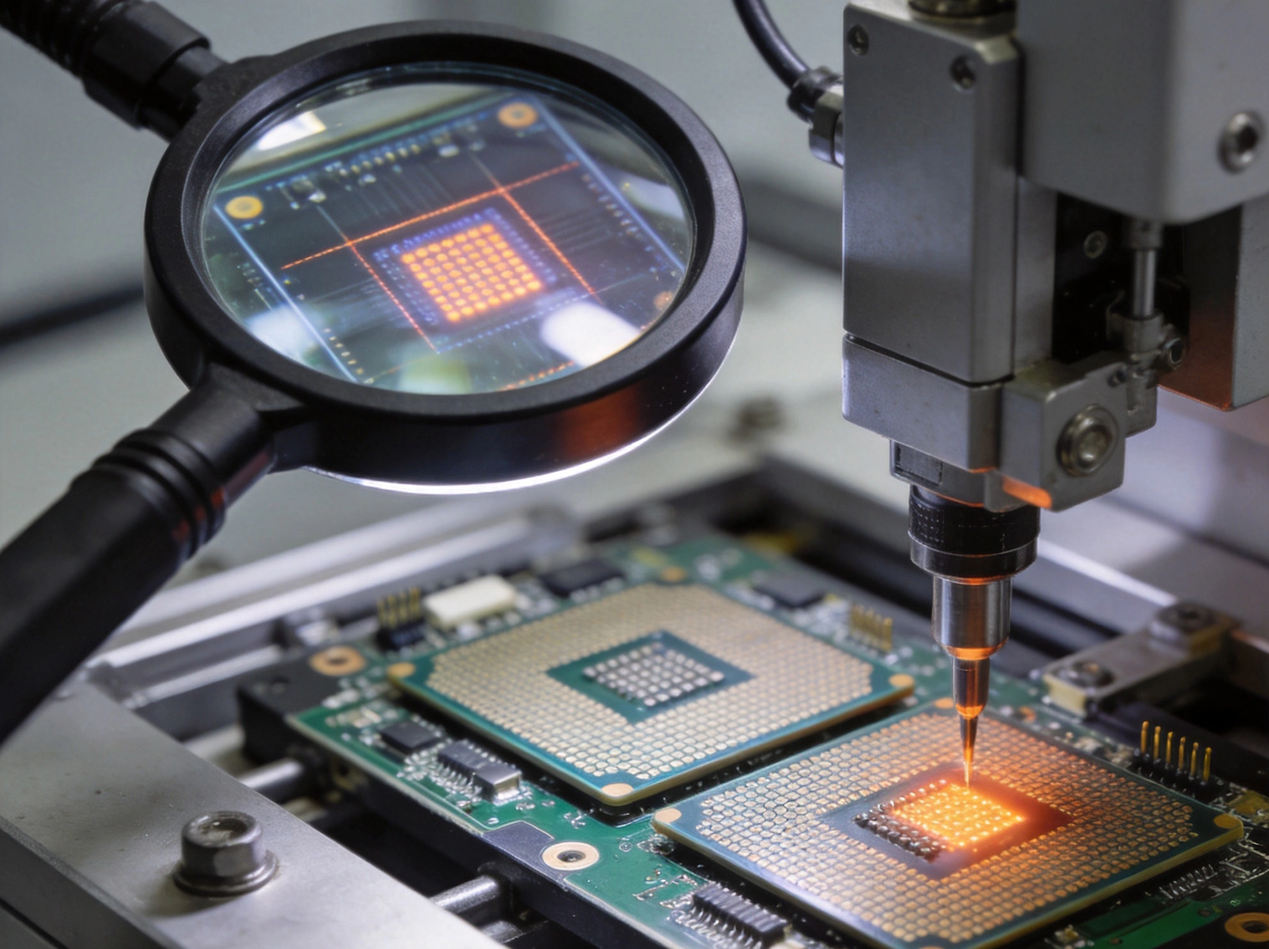
Troubleshooting Common Issues in HDI PCB Assembly September/09/2026 High Density Interconnect (HDI) printed circuit boards represent the pinnacle of miniaturization in electronics manufacturing. By utilizing microvias and fine-line geometries, HDI technology enables dramatically increased circuit density while reducing board size and weight. However, these same ch...
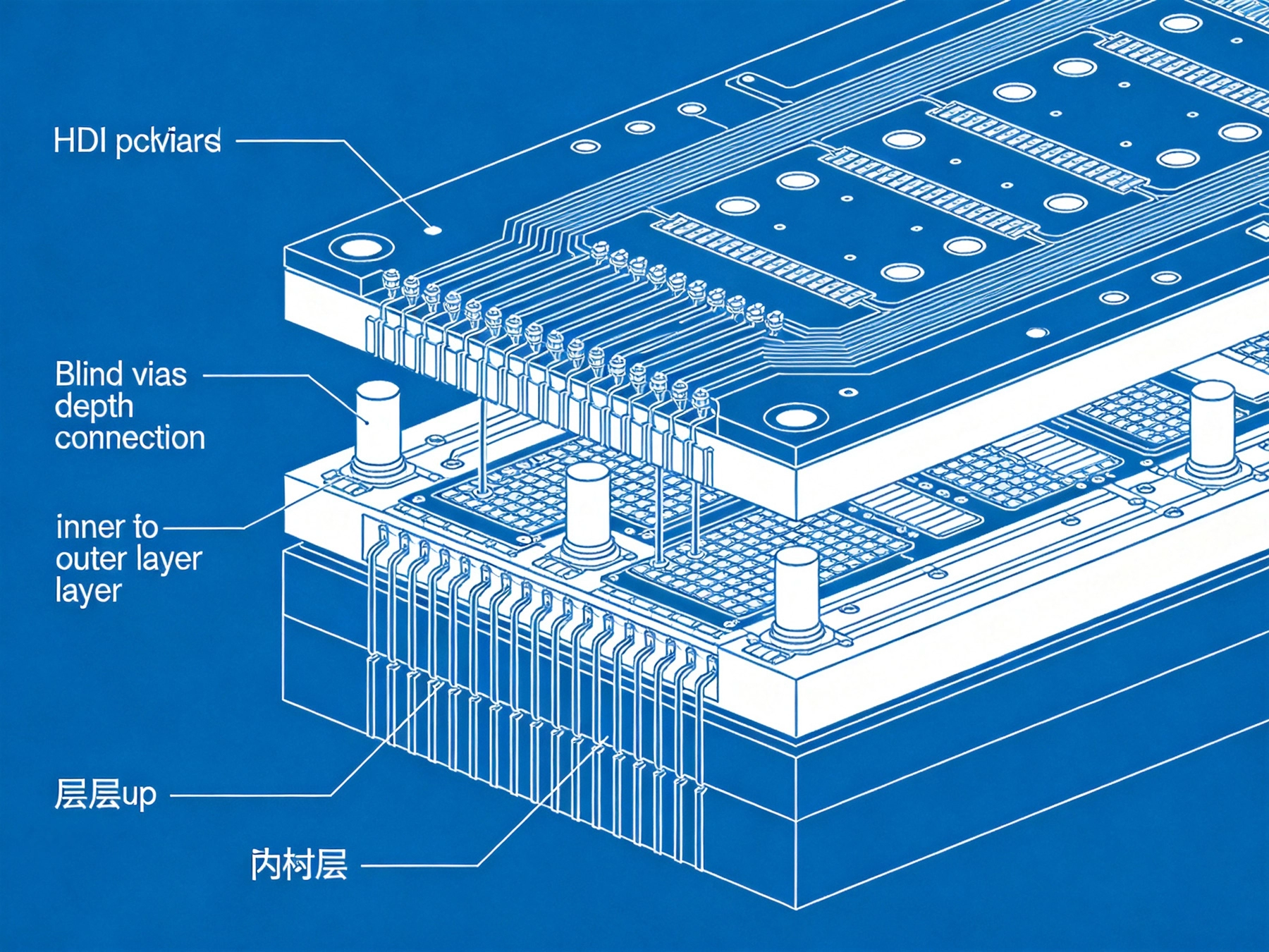
Understanding HDI Terminology: A Glossary for Engineers August/03/2026 High density interconnect (HDI) technology has revolutionized PCB design by enabling higher component density, smaller form factors, and improved electrical performance. However, the specialized manufacturing processes and design techniques associated with HDI have introduced terminology that can ...
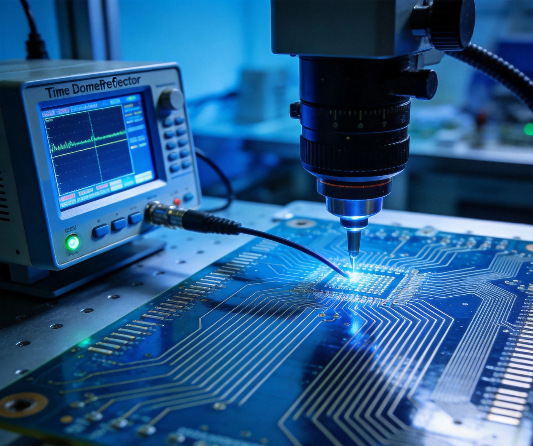
How to Measure and Control Impedance Tolerance in HDI Boards August/03/2026 High density interconnect (HDI) boards enable the miniaturization and performance requirements of modern electronics, but these benefits come with increased complexity in impedance control. As trace widths decrease, layer counts increase, and feature density rises, maintaining impedance within spe...
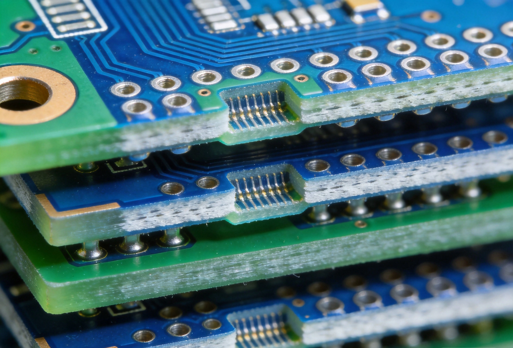
An Introduction to Microvia Technology in HDI PCBs July/24/2026 As electronics devices continue their relentless march toward miniaturization, the printed circuit boards inside them face increasing pressure to deliver more functionality in smaller footprints. High Density Interconnect (HDI) printed circuit boards, powered by microvia technology, have emerged a...
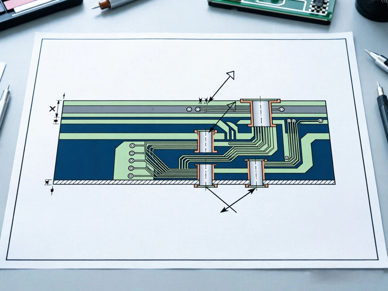
How to Read and Interpret HDI PCB Stack-up Drawings? July/14/2026 Misinterpreting HDI stack-up drawings causes manufacturing failures, design rejections, and expensive rework cycles. High-Density Interconnect (HDI) PCBs have become essential for modern electronics, enabling smaller form factors and higher functionality. But these advanced boards require soph...
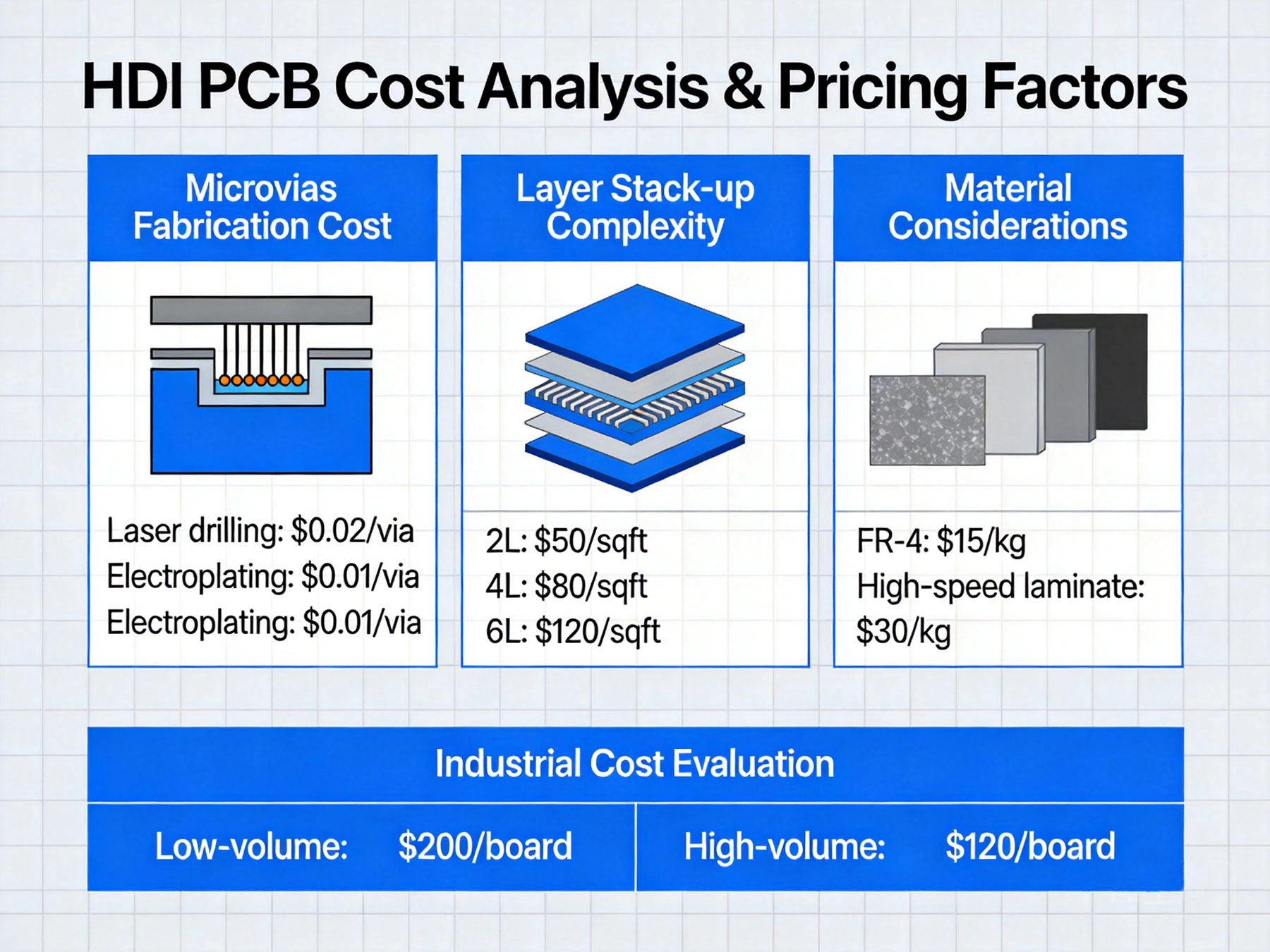
HDI PCB Cost Guide: What Factors Drive the Price Up? June/16/2026 Introduction: Understanding HDI PCB Pricing You've designed your product, specified HDI PCBs for the functionality you need, and requested quotes from manufacturers. The price comes back—often significantly higher than conventional PCBs. You might be wondering: why are HDI boards so expensi...

Implementing a Robust Quality Control System for HDI Manufacturing June/15/2026 High Density Interconnect (HDI) technology has revolutionized the electronics industry by enabling smaller, more powerful devices with advanced functionality. As HDI PCBs become increasingly complex with multiple layers, microvias, and fine-pitch components, the importance of implementing robust q...
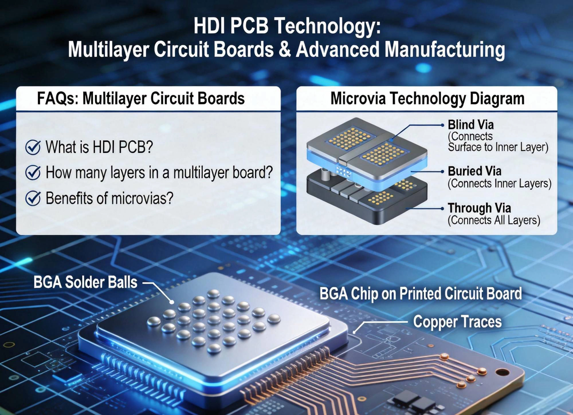
Top 10 Frequently Asked Questions About HDI PCB Technology May/28/2026 HDI PCB technology is one of the most transformative developments in electronics manufacturing of the past two decades. From smartphones and wearables to automotive ADAS systems and medical implants, HDI (High-Density Interconnect) PCB technology enables the miniaturization, performance, and funct...