
High-density Interconnect (HDI) technology has revolutionized Pcb Design by enabling unprecedented component density and Miniaturization. However, the very features that make HDI powerful, tightly packed components, fine-pitch traces, and buried Microvias, also create significant Thermal Management challenges. As power dissipation increases while available surface area for heat spreading decreases, thermal simulation has become an essential tool for ensuring HDI designs achieve both performance and reliability targets.
Thermal simulation software allows engineers to predict temperature distributions, identify hotspots, and optimize layouts before committing to expensive fabrication cycles. In Hdi Applications where design iterations carry substantial costs and schedule impacts, getting thermal design right the first time delivers measurable competitive advantages. Understanding how to effectively apply thermal simulation tools to HDI layouts separates designs that perform reliably from those that suffer thermal-induced failures in the field.
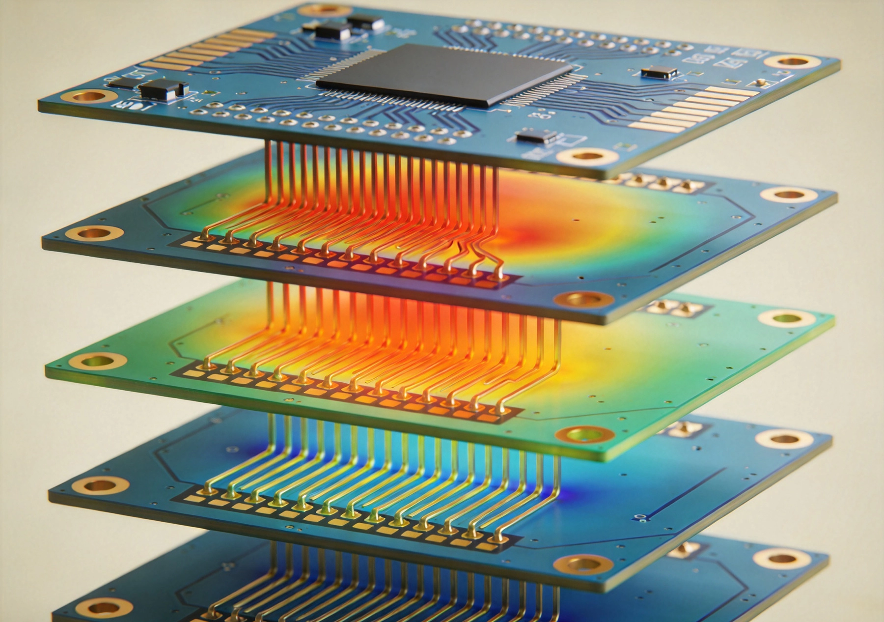
Hdi Technology presents unique Thermal Management challenges that differ fundamentally from standard PCB designs. The high component density typical of Hdi Boards concentrates heat sources in small areas, creating localized hotspots that can exceed component temperature ratings. Fine-pitch components with high power dissipation, such as processors, FPGAs, and power management ICs, generate substantial heat while occupying minimal board area, requiring efficient thermal paths to keep junction temperatures within specifications.
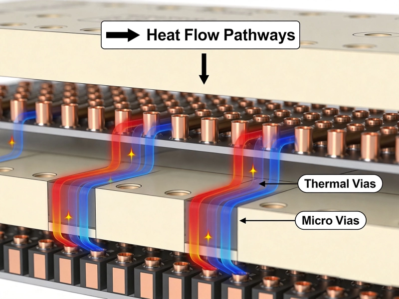
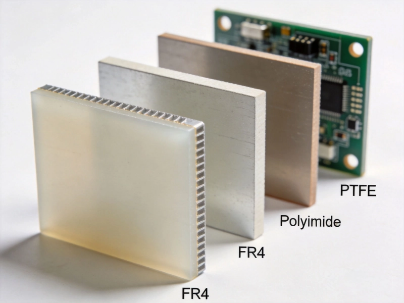
The multilayer structure of Hdi Boards, while enabling complex routing, can impede vertical heat flow. Buried and blind Microvias interrupt continuous copper planes that would otherwise spread heat efficiently. The dielectric materials between layers, typically FR-4 with Thermal Conductivity around 0.3 W/m·K, act as thermal insulators that limit heat spreading between layers. Without careful design, heat becomes trapped in the component layer, causing temperature rise that degrades performance and reliability.
Microvia density and placement also affect Thermal Performance. While microvias provide essential electrical connectivity between layers, their presence interrupts copper planes and can create thermal bottlenecks. The aspect ratio and fill material of microvias influence their effectiveness as thermal conduits. Unfilled or partially filled microvias offer limited Thermal Conductivity compared to solid copper structures, potentially creating high-resistance thermal paths.
Effective thermal simulation of HDI layouts requires understanding the physics of heat transfer and how simulation software models these phenomena. Conduction dominates heat transfer within the PCB itself, with heat flowing from hot components through copper traces, vias, and dielectric materials to cooler areas. Convection removes heat from the board surfaces to the surrounding air or cooling fluids, while radiation contributes a smaller but non-negligible heat transfer component at higher temperatures.
Computational Fluid Dynamics (CFD) software solves the governing equations for fluid flow and heat transfer, calculating temperature distributions throughout the PCB assembly. For Hdi Applications, CFD tools must resolve fine geometric features including microvias, trace widths down to 50 microns, and thin dielectric layers while also modeling the larger-scale system environment including enclosures, heat sinks, and airflow patterns. This multiscale modeling requirement makes HDI thermal simulation particularly challenging.
Boundary conditions significantly influence simulation accuracy. Ambient temperature, airflow velocity and direction, and surrounding component temperatures all affect the thermal solution. For natural convection cooling typical in many consumer electronics, accurate modeling of buoyancy-driven airflow requires careful attention to mesh resolution and solver settings. Forced convection systems with fans or liquid cooling introduce additional complexity through turbulence modeling and flow distribution effects.
Creating an accurate thermal simulation model begins with importing the Pcb Design data. Modern thermal simulation tools can import ECAD files directly from PCB design software, extracting component placement, copper layer geometries, and via structures. The ODB++ format provides comprehensive design data including layer stackup, net information, and component attributes that thermal tools use to build detailed geometric models.
Component modeling requires particular attention in HDI applications. Simple block models with uniform heat generation may suffice for low-power passives, but high-power ICs require detailed models that account for die size, package thermal characteristics, and internal heat spreading. Two-resistor thermal models provide a basic representation of junction-to-case and junction-to-board thermal resistances, while more sophisticated DELPHI models capture multi-path heat transfer through packages with greater accuracy.
Copper layer representation affects both electrical and thermal simulation accuracy. In HDI boards with fine-pitch traces, the detailed trace pattern influences local thermal conductivity. Some simulation tools offer trace-aware modeling that maps copper distribution onto thermal mesh elements, while others require simplified effective thermal conductivity values for copper layers. For critical applications, detailed copper geometry modeling captures the anisotropic thermal conductivity created by directional trace patterns.
Microvia modeling presents specific challenges due to their small size and high density. Explicitly modeling each microvia in a dense HDI board would create prohibitively large mesh counts. Instead, effective media approaches treat microvia fields as homogeneous materials with equivalent thermal properties derived from via density, fill material, and geometry. For critical thermal paths, detailed via modeling may be justified to capture local thermal resistance accurately.
Once the geometric model is established, defining operating conditions and power dissipation sets up the simulation scenario. Steady-state simulations calculate the equilibrium temperature distribution under constant operating conditions, providing the baseline Thermal Performance assessment. Transient simulations model temperature changes over time during power cycling or startup conditions, revealing thermal time constants and peak temperatures that steady-state analysis might miss.
Power dissipation values should represent realistic operating conditions rather than datasheet maximums. Many components dissipate varying power depending on operating modes, and worst-case scenarios may not represent typical usage patterns. For conservative design, simulations should include both typical and maximum power conditions to understand the full operating envelope.
Mesh generation balances solution accuracy against computational cost. HDI geometries with fine features require fine mesh resolution to capture thermal gradients accurately, but excessive mesh density increases solve time and memory requirements without improving results. Adaptive meshing techniques concentrate mesh elements in high-gradient regions while using coarser resolution in thermally uniform areas, optimizing the accuracy-to-cost ratio.
Solver settings control the numerical methods used to obtain thermal solutions. For natural convection problems, buoyancy effects and turbulence modeling require careful attention to solver stability and convergence criteria. Iterative solvers with appropriate relaxation factors ensure stable convergence for complex geometries, while direct solvers may be preferred for smaller, well-conditioned problems.
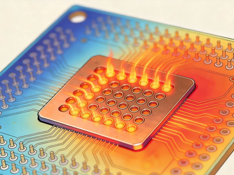
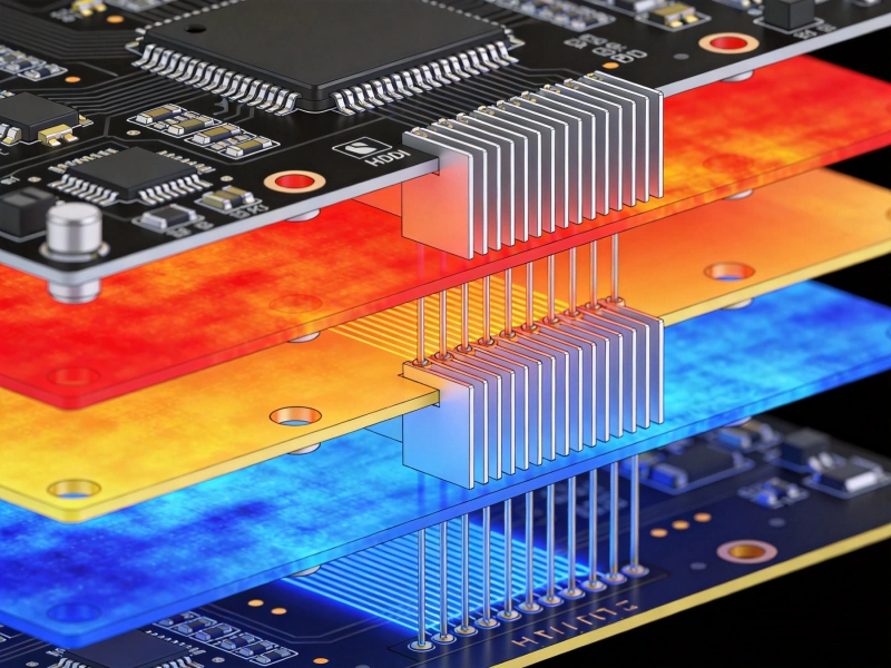
Post-processing transforms raw temperature data into actionable design insights. Temperature contour plots visualize hotspot locations and temperature gradients across the PCB surface. For HDI designs, these plots often reveal concentrated heating around processors or power components, with temperature falling off rapidly in surrounding areas due to limited heat spreading in densely routed regions.
Junction temperature predictions for critical components determine whether thermal specifications are met. Comparing predicted junction temperatures against maximum ratings with appropriate safety margins identifies components at risk of thermal failure. The temperature margin, typically 20 to 40 degrees Celsius below maximum ratings, provides headroom for manufacturing variations, aging effects, and extreme environmental conditions.
Thermal resistance paths reveal opportunities for layout optimization. Visualization tools can display heat flow vectors showing how heat moves from sources to sinks, highlighting thermal bottlenecks where high resistance limits heat removal. In HDI designs, these bottlenecks often occur at microvia transitions between layers or in areas with limited copper connectivity to ground or power planes.
Thermal simulation results guide targeted layout modifications to improve thermal performance. Component placement optimization spreads high-power devices across the board rather than clustering them, reducing localized heating. Thermal simulation quantifies the benefits of placement changes, helping designers balance thermal considerations against Signal Integrity, routing constraints, and form factor requirements.
Copper pour optimization enhances heat spreading from hot components. Adding Thermal Vias that connect component thermal pads to inner ground or power planes creates low-resistance paths for heat removal. Simulation validates the effectiveness of via placements, ensuring Thermal Vias are positioned where they provide maximum benefit without compromising Signal Integrity or manufacturability.
Trace routing adjustments can improve thermal performance without major layout changes. Widening power traces reduces resistive heating while also providing additional copper area for heat spreading. Strategic placement of ground plane connections creates thermal paths that supplement electrical connectivity. Thermal simulation quantifies the impact of these routing changes, enabling data-driven optimization decisions.
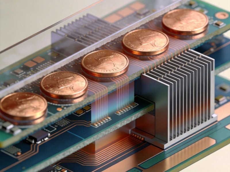
For designs with severe thermal constraints, advanced HDI features can be leveraged for thermal management. Stacked Microvias create denser thermal paths between layers than staggered configurations. Buried copper coins or embedded metal slugs in the PCB substrate provide high-conductivity thermal paths for extreme applications. Simulation validates these advanced thermal solutions before committing to the additional manufacturing complexity and cost they entail.
Heat generation in PCBs arises from electrical power dissipation, creating inherent coupling between electrical and thermal behavior. Iterative electro-thermal simulation captures this coupling by calculating temperature-dependent electrical properties and updating power dissipation based on actual operating conditions. For high-current HDI designs, this coupling is essential as resistive heating increases with temperature, creating potential thermal runaway conditions.
Temperature affects conductor resistance, with copper resistivity increasing approximately 0.4 percent per degree Celsius. In high-current traces, this resistance increase raises power dissipation, which further increases temperature. Without coupled electro-thermal analysis, simulation may underestimate temperatures and overestimate current-carrying capacity. Iterative simulation approaches alternate between electrical and thermal solutions until convergence, capturing these feedback effects accurately.
Semiconductor device characteristics also vary with temperature, affecting both power dissipation and timing. For digital circuits, leakage current increases exponentially with temperature, potentially dominating total power consumption at elevated temperatures. Thermal-aware power estimation using device models with temperature-dependent parameters provides accurate power inputs for thermal simulation, improving overall analysis accuracy.
Simulation accuracy should be validated against physical measurements to establish confidence in predictive capabilities. Infrared thermography provides non-contact temperature measurement across PCB surfaces, enabling direct comparison with simulation predictions. Thermocouples attached to component cases or board surfaces offer point measurements with high accuracy, though their presence may disturb the thermal field being measured.
Validation studies typically compare simulation predictions against measurements under controlled conditions with known power dissipation and boundary conditions. Discrepancies between simulation and measurement indicate areas where modeling assumptions require refinement. Common sources of discrepancy include inaccurate power estimates, simplified component models, or incorrect boundary condition specifications.
Correlation factors developed through validation studies can improve future simulation accuracy. If simulations consistently underpredict temperatures by a known margin, applying a safety factor accounts for modeling uncertainties. More sophisticated approaches adjust material properties or boundary condition coefficients to improve correlation across a range of operating conditions.
For HDI designs with extreme thermal challenges, advanced cooling solutions may be necessary. Heat sinks attached to high-power components increase surface area for convective heat transfer. Simulation evaluates heat sink effectiveness, optimizing fin geometry, spacing, and attachment methods for specific application constraints. Thermal interface materials between components and heat sinks introduce additional thermal resistance that must be accounted for in simulation models.
Forced convection with fans or blowers dramatically improves cooling capacity but introduces acoustic and reliability considerations. CFD simulation models airflow patterns through enclosures, identifying dead zones where cooling is ineffective and optimizing vent placement for uniform cooling. Fan selection based on airflow requirements and pressure drop characteristics ensures adequate cooling without excessive noise or power consumption.
Liquid cooling provides the highest heat removal capacity for extreme power densities. Cold plates with microchannel geometries offer compact cooling solutions that can be integrated into HDI assemblies. Two-phase cooling using vapor chambers or heat pipes provides high effective thermal conductivity with minimal volume, enabling thermal management in space-constrained applications where traditional solutions are impractical.
Successful thermal simulation of HDI layouts follows established best practices that ensure accuracy and efficiency. Early simulation in the design process allows thermal considerations to influence layout decisions before they become difficult to change. Integrating thermal simulation into the standard design workflow, rather than treating it as a final verification step, enables optimization rather than mere validation.
Sensitivity analysis identifies which parameters most strongly influence thermal performance. By varying power dissipation, material properties, and boundary conditions within expected ranges, engineers understand the robustness of thermal solutions and identify critical parameters requiring tight control. This understanding guides design decisions and test planning for prototype validation.
Parametric studies explore design trade-offs systematically. Automated simulation runs varying component placement, via density, or copper thickness generate response surfaces showing how thermal performance changes with design parameters. These studies reveal optimal design points that balance thermal performance against manufacturing cost and electrical performance requirements.
Documentation of simulation assumptions, boundary conditions, and results enables design knowledge capture and transfer. As designs evolve through product generations, accumulated thermal simulation data informs future design decisions and establishes corporate thermal design guidelines. This knowledge base accelerates future design cycles while maintaining consistent thermal quality.
Thermal simulation software has become an indispensable tool for Hdi Pcb design, enabling engineers to predict and optimize thermal performance in complex, high-density layouts. By modeling heat transfer physics with appropriate fidelity, executing simulations that capture operating conditions, and interpreting results to guide design decisions, thermal simulation transforms thermal management from a reactive Troubleshooting activity into a proactive design optimization process.
The investment in thermal simulation capability pays dividends through reduced prototype iterations, improved product reliability, and faster time-to-market. As Hdi Technology continues advancing toward higher densities and power levels, effective thermal simulation will only increase in importance. Engineers who master these tools and integrate thermal optimization into their design workflows will be best positioned to deliver successful HDI products that meet both performance and reliability requirements.
Managing Heat in High-Power HDI Applications: A Practical GuideSeptember/03/2026
Thermal Management Strategies for HDI Power ModulesSeptember/11/2026
Exploring the 6 Types of HDI Structures: From Type I to Any-LayerAugust/14/2026
The Role of Thermal Vias in Dissipating Heat from HDI BoardsJune/09/2026
Selecting the Right Dielectric Materials for High-Performance HDI PCBsMay/28/2026
The Impact of Via-in-Pad on Thermal Performance and ReliabilitySeptember/26/2026
Copper Coin and Embedded Heat Sinks: Advanced Cooling for HDIJuly/08/2026
Effective Thermal Management Strategies for High-Density PCBsMay/28/2026