Open Nav

High Density Interconnect (HDI) technology has become the backbone of modern electronics, enabling the Miniaturization that drives smartphones, wearable devices, and high-performance computing systems. At the heart of many advanced HDI constructions lies a specialized material called ABF—Ajinomoto Build-up Film. This epoxy-based Dielectric Material, developed by Ajinomoto Fine-Techno, has revolutionized how manufacturers build ultra-fine-pitch, high-layer-count boards that would be impossible with traditional construction methods. Understanding ABF's properties, applications, and limitations is essential knowledge for anyone working at the cutting edge of Electronics Packaging.
This article provides a comprehensive introduction to ABF technology, explaining what ABF is, how it works, why it matters for advanced Hdi Applications, and what design and manufacturing considerations you need to understand when using ABF-based construction. Whether you're a PCB designer tackling challenging Miniaturization requirements or an engineer evaluating material options for a new product, understanding ABF will expand your toolkit for solving modern Electronics Packaging challenges.
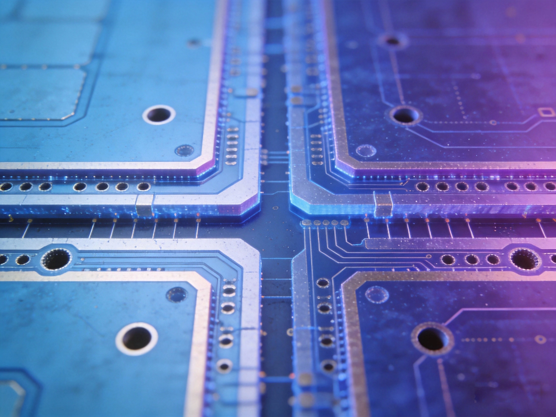
ABF is a photosensitive epoxy-based dry film material used in the build-up process for HDI PCBs. Unlike traditional liquid dielectric coatings that are applied and then cured, ABF is supplied as a pre-manufactured film that is laminated onto the board surface, exposed through a photomask, and developed to create the dielectric layer pattern. The material cures through a combination of thermal and photochemical processes, forming a solid, uniform dielectric layer with precisely defined openings where interconnections will be formed.
The chemistry of ABF combines epoxy resins with photoinitiators and specialized fillers that give the material its distinctive properties. The epoxy matrix provides dielectric strength, thermal stability, and mechanical rigidity. Photoinitiators enable controlled cross-linking when exposed to specific wavelengths of light. Fillers—typically inorganic particles—improve dimensional stability, reduce coefficient of thermal expansion, and enhance Thermal Conductivity. The specific formulation varies across ABF product lines, with different grades optimized for different applications and performance requirements.
ABF exists in multiple generations, each representing improvements in dielectric constant, Thermal Performance, and process capability. ABF-GX13, introduced in 2017, offered significant improvements in dielectric constant and loss tangent compared to earlier generations. ABF-GX93, released in 2019, further pushed performance with even lower dielectric constant (3.4-3.6) and improved thermal characteristics. The ongoing evolution of ABF technology reflects the relentless drive toward higher density, better electrical performance, and improved reliability in advanced electronics packaging.
ABF's advantages over alternative build-up materials stem from its specific combination of material properties. Understanding these properties helps designers and engineers understand when ABF is the appropriate choice and what performance to expect.
Dielectric constant (Dk) in ABF typically ranges from 3.4 to 4.0 depending on the specific grade, significantly lower than many conventional build-up materials. Lower Dk reduces signal propagation delay and improves Impedance Control in high-speed circuits—critical considerations for modern digital systems operating at multi-gigabit data rates. Loss tangent (Df) in ABF ranges from 0.006 to 0.015, providing low signal loss essential for high-frequency applications including 5G and mmWave communications.
Thermal Performance characteristics enable ABF to withstand the thermal stress of multiple reflow cycles. Glass transition temperature (Tg) typically exceeds 170°C in advanced ABF grades, providing comfortable margin above typical assembly temperatures. Thermal decomposition temperature (Td) exceeds 300°C, ensuring material stability during soldering processes. Coefficient of thermal expansion (CTE) in the XY plane—approximately 13-15 ppm/°C—matches reasonably well with copper, reducing thermal stress on plated through-holes and Microvias.
Mechanical properties support reliable board construction even with very thin dielectric layers. Modulus values in the range of 2.5-3.5 GPa provide sufficient rigidity for handling and processing while accommodating the thermal expansion mismatch between copper and dielectric. Peel strength—typically exceeding 10 N/cm—ensures reliable adhesion between ABF layers and copper foil, preventing delamination under thermal cycling and mechanical stress.
ABF's unique combination of properties enables HDI constructions that simply aren't feasible with alternative materials. The material addresses three fundamental challenges that limit how dense, fast, and reliable PCBs can become: dielectric thickness reduction, Microvia Reliability, and high-speed Signal Integrity.
Dielectric thickness in ABF builds can be as low as 15 microns in final copper-to-copper spacing, enabling dramatically reduced via pitch and improved routing density. Conventional epoxy glass prepregs typically cannot achieve uniform thickness below 50-75 microns, limiting how tightly Microvias can be spaced. ABF's ability to form consistently thin, uniform dielectric layers enables Microvia pitches below 0.2mm—the kind of density required for modern smartphone and tablet processors with thousands of connections in a compact footprint.
Microvia Reliability benefits from ABF's mechanical properties and its compatibility with advanced via formation processes. The material's low CTE reduces thermal stress on via barrels during thermal cycling. Its adhesion characteristics prevent delamination at the via-dielectric interface. Most importantly, ABF supports both laser-drilled and photodefined Microvia formation processes, giving manufacturers flexibility in how they create the interconnects that enable HDI density.
High-speed signal performance improves directly from ABF's electrical properties. Lower dielectric constant reduces propagation delay, supporting higher data rates and longer trace lengths before timing margins are exhausted. Lower loss tangent preserves Signal Integrity at high frequencies, reducing attenuation and maintaining signal quality through interconnects. For SERDES channels running at 25 Gbps and above, these electrical advantages can be the difference between a channel that meets specifications and one that doesn't.
ABF competes with several alternative build-up approaches, each with its own strengths and weaknesses. Understanding these alternatives helps clarify ABF's unique value proposition.
Liquid photoimageable dielectrics (PID) represent ABF's direct competitor for photoimageable build-up applications. PIDs offer similar capability for photodefined patterns but generally have higher dielectric constants and poorer thermal performance. Where PID materials typically exhibit Dk values of 4.0-4.5, ABF achieves 3.4-3.6—a significant improvement for high-speed applications. PID materials also typically have lower Tg and poorer thermal stability, limiting their use in applications subject to multiple reflow cycles or extended high-temperature operation.
Traditional prepreg-based build-up uses standard epoxy glass materials thinned through specialized processing to achieve thin dielectric layers. This approach can achieve very thin dielectrics but at substantial cost and with significant process limitations. The uniformity of thickness suffers compared to film-based approaches, and the inability to photodefine via openings requires separate Laser Drilling steps. For volume production, prepreg-based build-up is generally more expensive and less capable than ABF-based approaches for advanced Hdi Applications.
Ceramic-filled polymer systems offer improved Thermal Conductivity and reduced CTE compared to standard epoxy materials, potentially making them attractive for high-power applications. However, these materials typically have higher dielectric constants than ABF and often require specialized processing that adds cost and complexity. For most high-speed digital applications, ABF's superior electrical properties outweigh the thermal advantages of ceramic-filled alternatives.
The process flow for ABF-based HDI construction differs from conventional Pcb Manufacturing in several important respects. Understanding this process helps designers understand the constraints that affect their designs and helps manufacturing engineers optimize production yields.
The process begins with a copper-clad substrate that may already contain core layers and through-holes. ABF film is laminated onto the copper surface using heat and pressure, bonding the film to the copper and creating a uniform dielectric layer. Lamination parameters—temperature, pressure, and dwell time—must be controlled carefully to achieve consistent thickness and prevent entrapped air or voids that would create defects.
After lamination, the ABF layer is exposed through a photomask that defines the pattern for dielectric removal. The photomask contains clear areas where dielectric will be removed to create via openings and opaque areas where dielectric will remain. The exposure wavelength and energy must be controlled precisely to achieve complete curing in exposed areas without affecting the material under the mask. Modern ABF processing uses broadband UV exposure with carefully controlled energy density.
Development follows exposure, dissolving the unexposed ABF to create the dielectric openings. The development chemistry and time must be optimized to achieve clean sidewalls and complete removal of unexposed material without undercutting the exposed areas. Overdevelopment increases via diameter beyond the intended size; underdevelopment leaves residual material that prevents proper via formation. Precise process control at this step is critical for dimensional accuracy.
Desmear and metallization prepare the dielectric openings for Copper Plating. A plasma desmear process removes any residual polymer material from the via sidewalls and improves adhesion for subsequent metallization. A thin seed layer of copper is deposited through electroless plating, followed by copper electroplating that builds up the copper thickness in the vias and on the surface. The plating process must fill the high-aspect-ratio microvias completely without creating voids or trapped plating solution.
The process described above repeats for each build-up layer in an ABF-based HDI construction. A typical 1+N+1 construction (one signal layer, N build-up layers, one signal layer) might require 4-8 build-up cycles to achieve the full layer stackup. Each cycle adds another ABF layer with its own microvias and circuit patterns, progressively building up the interconnect density.
The sequential build-up process creates registration challenges—each new layer must align precisely with all previous layers. Registration accuracy of ±15 microns or better is typically required to ensure microvias land correctly on target pads across the entire build-up stack. This requirement drives manufacturing equipment investment and process control sophistication. The most advanced ABF-based Hdi Manufacturing uses laser-based direct imaging systems that achieve registration accuracy approaching ±5 microns.
Process yield considerations drive layer count decisions. Each build-up layer introduces opportunities for defects, and cumulative yield across multiple build-up layers can become unacceptably low for very high layer counts. Manufacturers must balance the design's layer count requirements against the economic realities of cumulative yield loss. This constraint often drives designs toward the minimum layer count that meets routing requirements rather than pursuing maximum density regardless of cost.
Designing for ABF-based construction requires understanding the material's capabilities and limitations and designing to leverage the strengths while avoiding the weaknesses. Several key design considerations distinguish ABF-based designs from conventional PCB designs.
Microvia dimensions in ABF construction must respect manufacturing capabilities. Minimum via diameter typically ranges from 50-75 microns depending on the specific ABF grade and manufacturer's process capabilities. Minimum land diameter typically exceeds via diameter by 80-100 microns to ensure reliable plating and adequate current-carrying capacity. Via pitch—the center-to-center spacing between adjacent vias—must account for both via diameter and land size, with typical minimum pitch ranging from 150-200 microns for the most advanced processes.
Aspect ratio limitations constrain the relationship between via depth and via diameter. Deep, narrow vias are difficult to plate reliably without creating voids. In ABF constructions, aspect ratio typically remains below 1:1—meaning via depth should not exceed via diameter. This constraint affects how many build-up layers can be stacked before microvia stubs become problematic, potentially requiring backdrilling or filled via strategies to maintain signal integrity in high-speed applications.
Impedance Control in ABF-based designs must account for ABF's dielectric properties and the thin dielectric layers that characterize ABF constructions. Lower dielectric constant means wider traces achieve the same impedance compared to materials with higher Dk. The dielectric constant of ABF also varies slightly with frequency—typically increasing 5-10% from 1 MHz to 10 GHz—which must be accounted for in impedance calculations for high-frequency applications.
The thin dielectric layers possible with ABF affect differential pair spacing and coupling. With very thin dielectrics between signal layers, interlayer coupling becomes significant, potentially affecting crosstalk and impedance. Designers must use 3D electromagnetic field solvers rather than simple 2D calculators to accurately predict impedance and coupling in ABF-based multilayer structures.
Thermal Management in ABF-based designs must account for ABF's thermal conductivity, which is relatively low compared to metal core boards or specialized thermal materials. Heat spreading through ABF layers is limited, so Thermal Vias—staggered arrays of plated through-holes—become critical for conducting heat from hot components into inner plane layers or external heat sinks. Thermal via design in ABF constructions faces the same aspect ratio limitations as signal vias, requiring careful planning to achieve adequate thermal paths without exceeding manufacturing capabilities.
ABF's CTE, while reasonably matched to copper, still creates thermal stress on vias and through-holes during thermal cycling. Designs that will undergo significant temperature swings—automotive under-hood applications, outdoor equipment, or products with substantial internal power dissipation—must incorporate design features that reduce thermal stress. Symmetrical layer stackups, balanced copper distribution, and avoidance of concentrated copper mass all help reduce CTE-related stress.
ABF technology finds application across a range of high-performance electronics packaging requirements where miniaturization, speed, or both are critical design drivers.
Mobile devices—smartphones, tablets, and wearable technology—represent the largest application for ABF-based HDI. The relentless drive toward thinner, lighter, more powerful mobile products requires PCBs with exceptional density in compact form factors. ABF enables the microvia pitch and layer counts needed to route the thousands of connections required for modern application processors in the limited board area available in mobile devices. The electrical performance characteristics of ABF also support the multi-gigabit data rates required for mobile data interfaces.
High-performance computing systems—including servers, workstations, and AI accelerators—leverage ABF's electrical performance advantages. SERDES channels running at 25 Gbps and beyond require low-loss dielectrics to maintain signal integrity over the channel lengths found in large computing platforms. ABF's low loss tangent and controlled dielectric constant enable these high-speed interconnects with adequate margin for signal integrity and timing closure.
Advanced packaging—including 2.5D and 3D package-on-package structures—uses ABF as the build-up material in the interposer or substrate. The fine pitch, thin dielectrics, and reliable via formation that ABF provides make it suitable for the extremely demanding requirements of advanced packaging. As chip-to-chip interconnects shift toward higher density and higher speed, ABF-based substrates become increasingly important enablers of these packaging technologies.
5G wireless and millimeter wave applications particularly benefit from ABF's electrical properties. At frequencies above 24 GHz, Dielectric Loss becomes a dominant factor in signal attenuation. ABF's low loss tangent—typically 0.006-0.015 at 10 GHz, with even better performance at higher frequencies—minimizes this loss, preserving signal strength and enabling practical antenna-in-package and front-end module designs that would be impractical with higher-loss dielectrics.
The dimensional control achieved with ABF photopatterning supports the tight geometries required for millimeter wave circuits. Antenna elements, transmission lines, and transitions require precise dimensions to achieve target impedance and radiation patterns. ABF's photodefinable capability, combined with advanced imaging systems, enables the ±10 micron dimensional control that millimeter wave designs demand.
Despite its advantages, ABF is not universally appropriate for all PCB applications. Understanding its limitations helps avoid inappropriate material selection.
Cost remains a significant factor. ABF-based HDI construction costs substantially more than conventional PCB construction due to multiple sequential build-up cycles, expensive imaging systems, and lower overall process yields. For applications where density and high-speed performance are not critical requirements, alternative materials and construction methods provide more economical solutions.
Thermal conductivity limitations make ABF less suitable for high-power applications where Heat Dissipation through the substrate is critical. While ABF performs adequately for typical digital and RF applications, boards carrying high currents or dissipating substantial power may benefit from metal-core constructions or specialized high-thermal-conductivity materials despite the electrical performance advantages of ABF.
Design complexity increases dramatically with ABF-based HDI. The very capabilities that enable high density—ultra-fine-pitch microvias, thin dielectrics, high layer counts—also make designs more challenging to route, more difficult to manufacture, and more sensitive to design errors. Companies considering ABF-based designs should ensure they have access to design expertise and design automation tools capable of handling HDI complexity.
The practical minimum copper-to-copper dielectric thickness in ABF constructions is approximately 15 microns, achieved with the thinnest ABF grades and optimized processing. Theoretical minimums are even lower, but below approximately 15 microns, manufacturing yield decreases and process control becomes extremely challenging. Most manufacturers recommend 20-25 microns as a practical minimum for volume production. The dielectric thickness affects via drill depth and aspect ratio, so minimum thickness considerations must be balanced against via design requirements.
Manufacturers routinely build 4-8 build-up layers on each side of a core substrate, creating total layer counts of 10-20 layers. Beyond approximately 8 build-up layers per side, cumulative yield loss and registration challenges make additional layers increasingly impractical. The most complex production boards with ABF typically achieve approximately 18-20 total layers. Experimental demonstrations have exceeded 30 layers, but these remain impractical for most commercial applications due to cost and yield considerations.
Yes, hybrid constructions combining ABF build-up layers with Rogers or other high-frequency core materials are common in advanced RF applications. The Rogers core provides the electrical characteristics required for RF signal propagation, while ABF build-up layers provide the fine-pitch interconnect density required for component packaging. The transition between ABF and Rogers laminates requires careful process planning to ensure reliable bonding between the dissimilar materials, but hybrid constructions represent a proven approach for complex RF-digital mixed-signal designs.
ABF exhibits moisture absorption characteristics similar to conventional epoxy-based laminates, typically absorbing 0.10-0.15% by weight under standard conditions. This moisture content must be managed through proper storage conditions and baking before lamination to prevent delamination during thermal processing. Moisture sensitivity classification (MSL) for ABF-based boards is typically MSL 3, requiring baking before assembly if exposed to ambient humidity for extended periods. Moisture management procedures for ABF are similar to those for standard FR4 materials.
Yes, ABF materials are specifically formulated to withstand the higher temperatures of lead-free soldering. With Tg values typically exceeding 170°C and Td values exceeding 300°C, ABF provides adequate thermal margin for lead-free reflow profiles that peak at 250-260°C. The material's thermal stability and mechanical strength at elevated temperatures prevent softening, delamination, or other thermal failures during lead-free assembly. ABF has been qualified for lead-free processes in major Electronics Manufacturing environments.
ABF technology represents one of the key enablers of modern electronics miniaturization and high-speed performance. By providing a unique combination of low dielectric constant, low loss tangent, thin dielectric capability, and reliable microvia formation, ABF makes possible the HDI constructions that power today's most advanced electronic devices. From smartphones to AI accelerators to 5G infrastructure, ABF-based HDI provides the interconnect density and electrical performance that cutting-edge electronics demand.
The decision to use ABF involves trade-offs: higher cost and increased complexity in exchange for superior density and performance. For applications where these advantages matter—mobile devices, high-performance computing, advanced packaging, and high-frequency wireless systems—the trade-off typically favors ABF. For applications where density and high-speed performance are not critical requirements, alternative materials and construction methods provide more economical solutions.
As electronics continue their march toward greater integration, higher speed, and smaller form factors, ABF and similar advanced build-up materials will play increasingly important roles in enabling these advances. Understanding ABF technology—its capabilities, limitations, and design considerations—positions engineers and designers to leverage these materials effectively, creating the next generation of electronic products that push the boundaries of what's possible in electronics packaging.
Considering ABF-based HDI for your next design? Our engineering team specializes in Advanced Pcb technologies including ABF-based construction. Contact us for a design review and manufacturing feasibility assessment for your specific requirements.
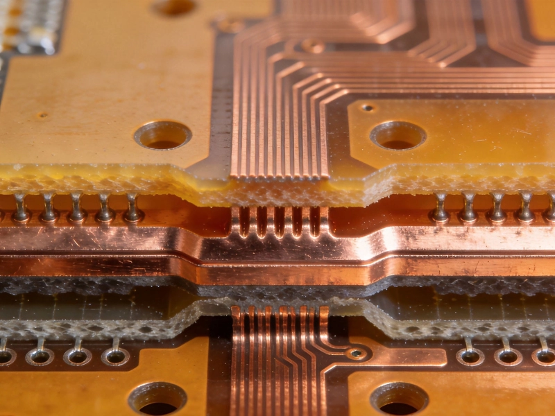
d-0-64486247a54c1de02841b54d695fa65b7e6795ed20040acb4f4851f63c9d9015" alt="Microscopic cross-sectional view of ABF build-up film layers in Hdi Pcb structure" />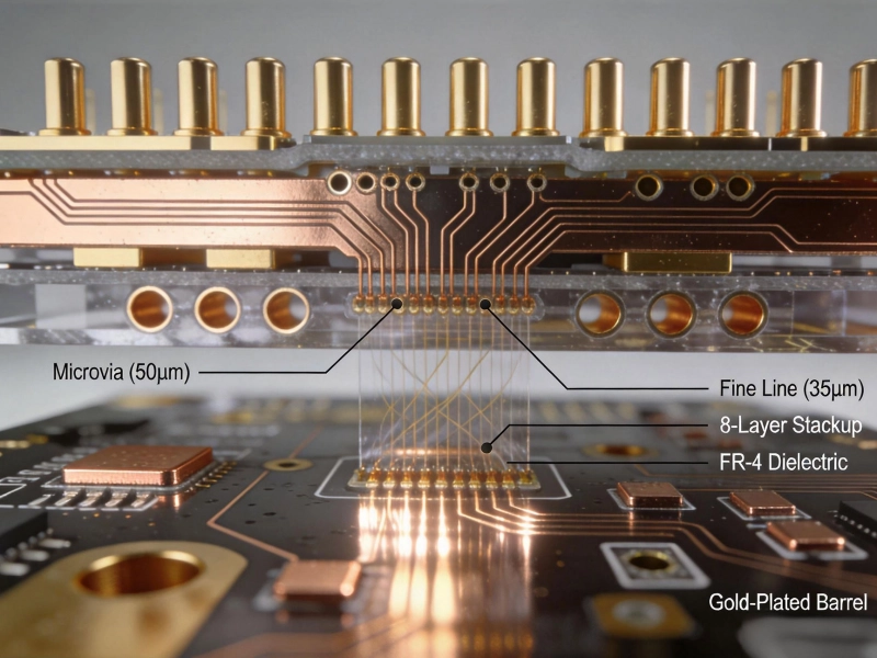
What is High Density Interconnect (HDI) PCB?May/28/2026
Managing Layer-to-Layer Registration Accuracy in Multilayer HDIOctober/09/2026
Selecting the Right Dielectric Materials for High-Performance HDI PCBsJune/05/2026
FR-4 vs. High-Tg Materials: What Works Best for HDI Applications?July/07/2026
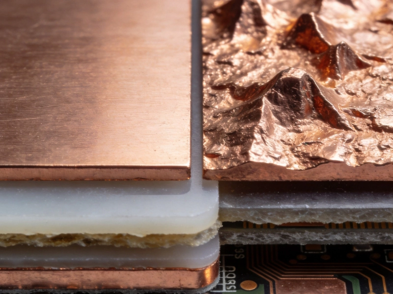
Understanding the Role of Copper Foil Roughness in Signal IntegritySeptember/23/2026
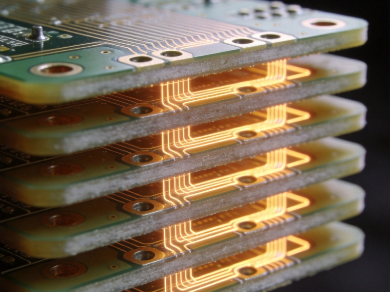
Why Low Loss Materials are Critical for High-Speed HDI DesignsSeptember/01/2026
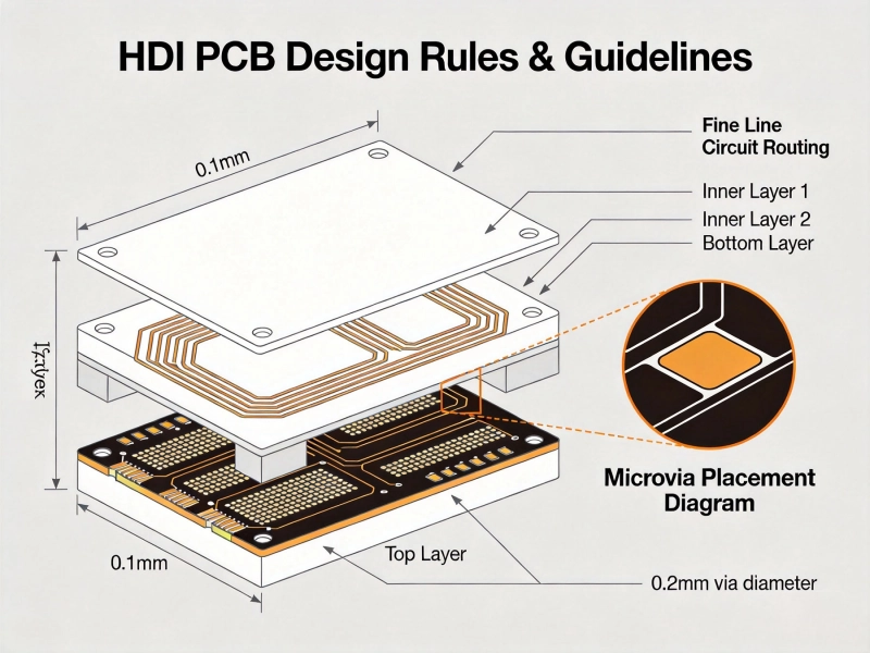
Essential HDI PCB Design Rules for Beginners and ExpertsMay/28/2026
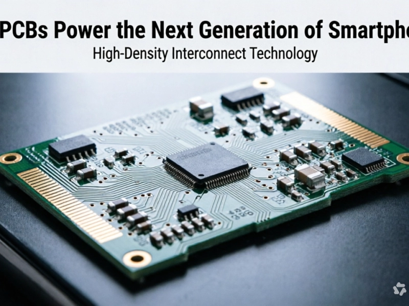
How HDI PCBs Power the Next Generation of SmartphonesJune/17/2026