
The printed circuit board—the unassuming green board that powers virtually every electronic device in our modern world—has undergone one of the most remarkable technological transformations in manufacturing history. From humble beginnings as simple single-sided boards to today's sophisticated High-density Interconnect (HDI) structures, the evolution of Pcb Technology mirrors the broader story of electronics Miniaturization and performance advancement.
Understanding this evolution provides valuable context for engineers, designers, and decision-makers working with electronic systems today. The challenges faced and solutions developed over decades of innovation inform best practices, reveal fundamental trade-offs, and point toward future developments in electronic packaging.
This comprehensive exploration traces the journey from standard multilayer PCBs to Hdi Technology, examining the driving forces, key innovations, and ongoing evolution that continues to shape how we build electronic systems.
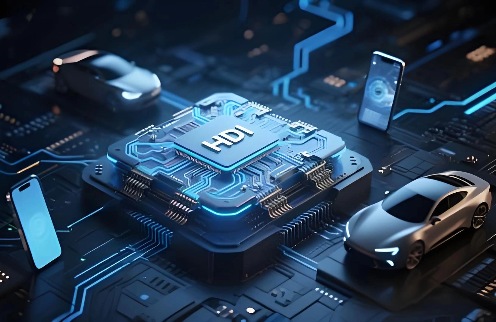
To appreciate how far Pcb Technology has come, we must first understand where it began. The printed circuit board concept dates back to the early 20th century, with the first commercially manufactured PCBs appearing in the 1940s and 1950s for military and early computing applications.
Early PCBs were primitive by today's standards:
These early boards solved critical problems of reliability and manufacturability for electronic assemblies, replacing bundles of hand-soldered wires with consistent, repeatable connections.
The introduction of double-sided PCBs marked a significant advancement:
Double-sided boards remain widely used today for many applications, demonstrating that sometimes simpler solutions are the most appropriate.
As electronic systems grew more complex, double-sided boards reached their routing limits. The introduction of multilayer PCBs in the 1960s opened entirely new possibilities for electronic design.
Multilayer boards emerged from military and aerospace requirements:
Early multilayer boards were expensive and challenging to manufacture, limiting their use to high-value applications. As processes improved, costs decreased and applications expanded.
Standard multilayer PCBs consist of multiple layers of substrate material laminated together:
Typical multilayer boards range from 4 to 12 layers for commercial applications, with specialized boards reaching 50 layers or more for the most demanding applications.
Multilayer boards provided transformative benefits:
Multilayer manufacturing processes continuously improved over decades:
These improvements enabled higher layer counts, tighter tolerances, and lower costs—expanding multilayer applications from aerospace to consumer electronics.
Despite continuous improvement, traditional multilayer technology faced fundamental limitations as electronics Miniaturization accelerated.
Traditional multilayer boards have inherent density limitations:
As consumer electronics demanded smaller, lighter products:
Traditional Pcb technology could not efficiently meet these requirements. Something fundamentally different was needed.
High-density Interconnect (HDI) technology emerged in the 1990s as a solution to the limitations of traditional multilayer boards. HDI represents not merely an incremental improvement but a paradigm shift in how PCBs are designed and manufactured.
Hdi Technology is defined by several key characteristics:
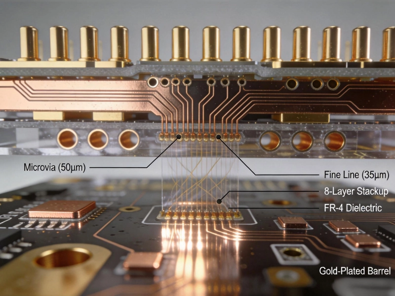
The Microvia is the cornerstone of HDI technology:
Hdi Boards use sequential build-up rather than traditional lamination:
HDI technology required development of entirely new manufacturing capabilities.
Laser Drilling enabled the Microvia revolution:
HDI requires materials optimized for laser processing:
Build-up layers require excellent surface flatness:
Understanding the differences between traditional multilayer and HDI technology helps designers select the appropriate approach for each application.
| Feature | Traditional Multilayer | HDI |
|---|---|---|
| Via diameter | 200-300+ microns | 50-150 microns |
| Trace width | 100-150 microns typical | 50-75 microns typical |
| Minimum pitch | 400-500 microns | 200-300 microns |
| Layer count | 4-50+ layers | 2-12 layers typical |
| Via aspect ratio | Up to 10:1 or higher | Typically 1:1 or less |
Cost Comparison:
Several application areas have driven aggressive HDI adoption and continuous capability advancement.
Mobile phones represent the most demanding HDI application:
Smartphone competition has driven HDI capability advancement faster than any other sector.
Wearable devices push HDI in new directions:
Implantable and portable medical devices benefit from HDI:
Modern vehicles increasingly rely on HDI:
HDI technology continues to evolve, with new approaches pushing the boundaries of electronic packaging.
The next generation of miniaturization blurs lines with semiconductor packaging:
HDI increasingly integrates with other packaging approaches:
New materials enable new capabilities:
Designing with HDI requires different approaches than traditional multilayer boards.
HDI design operates under different constraints:
HDI benefits from early manufacturer involvement:
HDI should be used where its benefits justify the cost:
Looking ahead, PCB technology will continue evolving to meet demanding requirements.
Environmental concerns drive new approaches:
Emerging applications push performance boundaries:
The evolution of PCB technology from simple single-sided boards through standard multilayer to today's HDI technology represents one of the most significant technological journeys in manufacturing history. Each advancement responded to real market needs: more functionality, smaller size, better performance, and lower cost.
Traditional multilayer PCBs remain essential for countless applications where their capabilities are fully adequate. HDI technology shines where miniaturization, performance, and density requirements exceed what traditional technology can efficiently provide. The art of electronic design lies in selecting the appropriate technology for each specific application.
As electronic systems continue to advance—driven by artificial intelligence, autonomous vehicles, wearable technology, and the Internet of Things—PCB technology will continue evolving to meet these demands. The foundations laid by decades of innovation provide the platform for future breakthroughs in electronic packaging.
Understanding this evolution helps designers appreciate the capabilities and limitations of each technology, enabling informed decisions that balance performance, cost, and manufacturability. Whether you're working with traditional multilayer boards or cutting-edge HDI, the principles remain the same: design for your application, understand your manufacturing options, and build partnerships that enable success.
Traditional multilayer PCBs use mechanically drilled through-hole vias (200-300+ microns diameter) with traces typically 100-150 microns wide. HDI PCBs use laser-drilled microvias (50-150 microns diameter) with traces as narrow as 50-75 microns. HDI enables significantly higher component density but at higher manufacturing cost per unit area.
Choose HDI when your design requires high component density in a limited area, benefits from shorter signal paths for high-speed performance, needs to minimize board size or weight, or requires advanced packaging approaches like embedded components. Use traditional multilayer when density requirements are modest and cost sensitivity is high.
HDI typically costs 20-50% more per unit area than equivalent traditional multilayer boards. However, HDI often reduces total system cost by enabling smaller form factors, fewer boards in a system, and simplified assembly. Evaluate total system cost rather than PCB unit cost alone.
Any-layer HDI allows microvias to connect any two adjacent layers throughout the board, providing maximum routing flexibility. This approach is used in the most demanding applications like flagship smartphones where density requirements are extreme. Standard HDI may connect only outermost layers to the core, which is sufficient for many applications at lower cost.
The future includes substrate-like PCBs (SLP) with semiconductor-like feature sizes, increased integration of embedded components and bare die, advanced materials like glass substrates, and continued evolution toward system-in-package approaches. PCB technology will remain essential even as it blurs boundaries with semiconductor packaging.
The Role of HDI PCBs in Miniaturized Implantable Medical DevicesJuly/21/2026
How X-Ray Inspection (AXI) Detects Hidden Defects in HDI BoardsJuly/30/2026
What is High Density Interconnect (HDI) PCB?May/28/2026
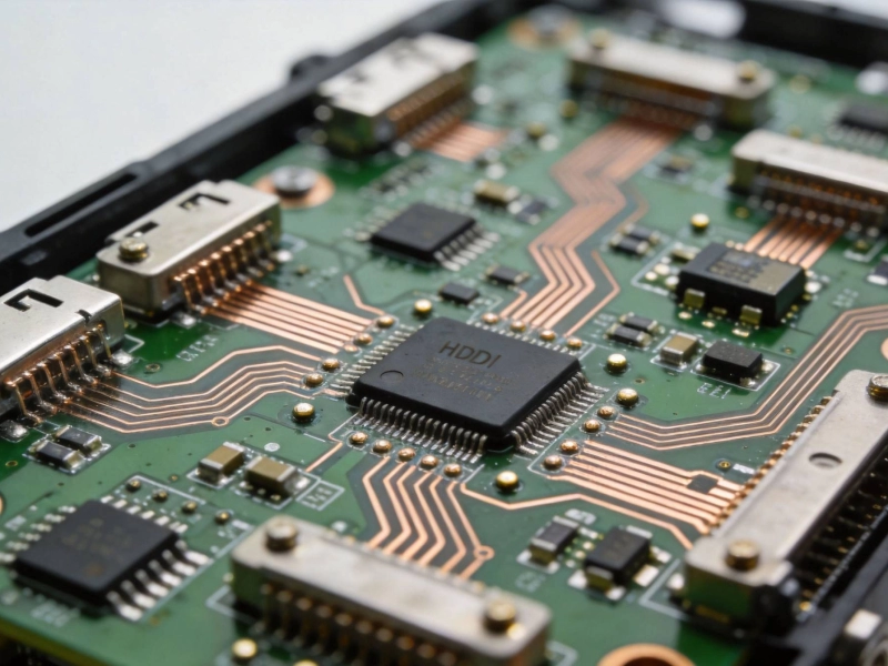
HDI Applications in Advanced Battery Management Systems (BMS)June/18/2026
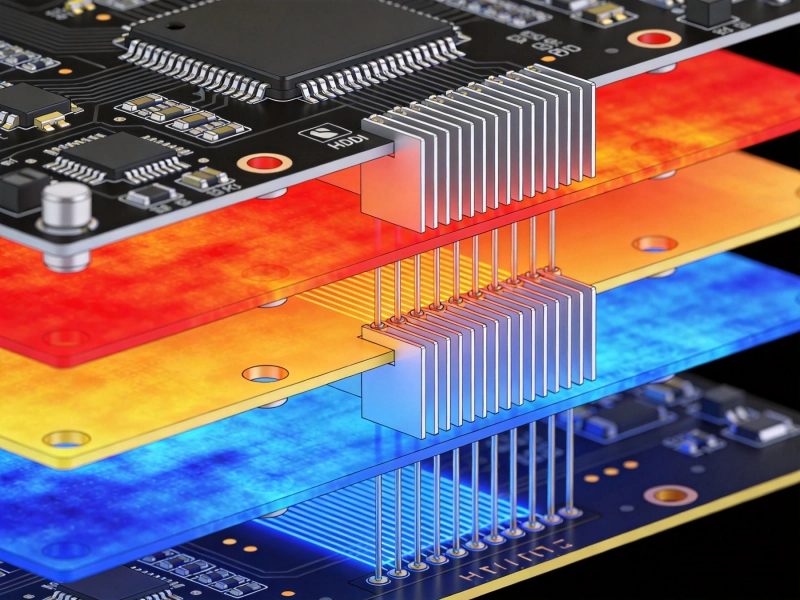
Effective Thermal Management Strategies for High-Density PCBsMay/28/2026
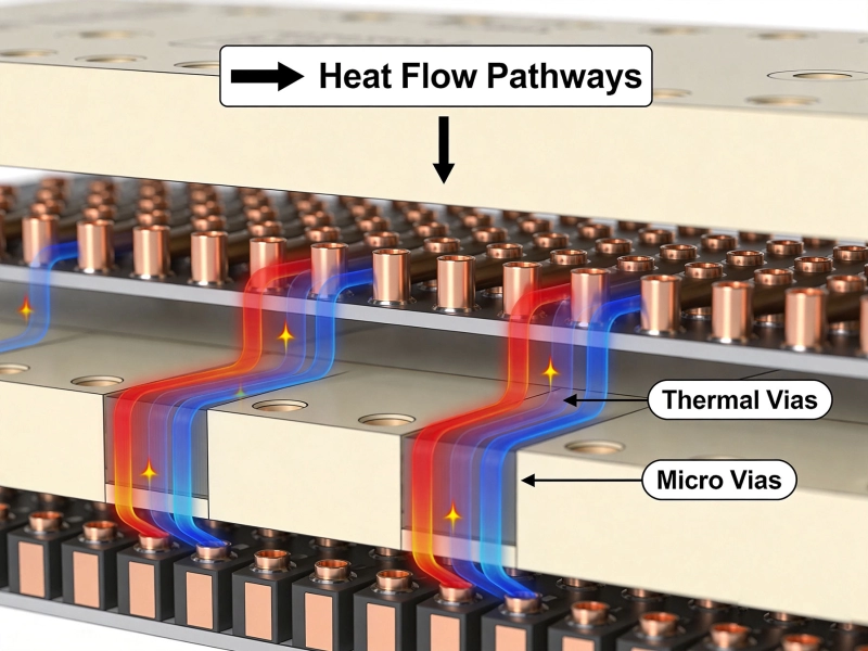
The Role of Thermal Vias in Dissipating Heat from HDI BoardsJune/09/2026
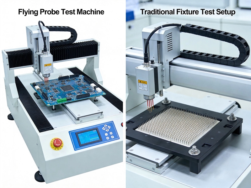
Flying Probe vs. Fixture Testing: Which is Best for HDI PCBs?June/11/2026
Designing for Manufacturing (DFM): Avoiding Common HDI PitfallsSeptember/02/2026