
Medical implantable devices have undergone a remarkable transformation. Early pacemakers were the size of hockey pucks, implanted in abdominal pockets. Modern cardiac devices are smaller than a coin, yet deliver more sophisticated therapy. Cochlear implants have shrunk from external processors to partially implanted systems. Neurostimulators target increasingly specific neural pathways. This Miniaturization revolution would be impossible without corresponding advances in printed circuit board technology.
High Density Interconnect (HDI) PCBs have emerged as the enabling technology for next-generation implantable medical devices. By allowing more circuitry in less space, supporting finer-pitch components, and providing the reliability that life-critical applications demand, Hdi Technology makes possible devices that were inconceivable just decades ago.
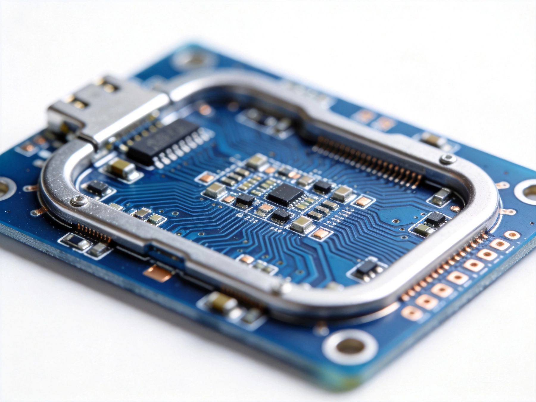
Understanding why Miniaturization matters clarifies why Hdi Technology has become essential.
Smaller implants cause less surgical trauma. A coin-sized device requires a smaller incision, reduces post-operative pain, and enables faster recovery. For devices implanted near sensitive anatomy—a neurostimulator near the spine, a cochlear implant near the ear—size reduction directly improves patient outcomes.
Smaller devices are also less noticeable. For patients wearing medical devices, discretion affects psychological acceptance and quality of life. A subcutaneous neurostimulator that doesn't create a visible bulge allows normal activities without self-consciousness.
Some implantation sites simply cannot accommodate large devices. Deep brain stimulators must fit within limited cranial space. Cochlear implants must navigate the intricate anatomy of the temporal bone. Cardiovascular implants must work within blood vessels or heart chambers. These anatomical constraints create hard limits on device size.
Miniaturization enables applications that larger devices cannot serve. Smaller devices can reach new anatomical locations. The same therapy can be delivered with less invasive procedures. New applications emerge as devices shrink—from neurological monitoring to drug delivery to physiological sensing.
Smaller electronics often consume less power, extending battery life or enabling smaller batteries. For implantable devices where battery replacement requires surgery, extended service life represents a significant clinical benefit. Some miniaturized devices can even operate on harvested energy, eliminating batteries entirely.
HDI PCBs achieve higher density through technologies not found in conventional PCBs.
Microvias are the defining feature of HDI construction. These small vias—typically 0.15mm or less in diameter—enable connections between fine-pitch components and inner layer circuitry. Unlike mechanically drilled vias, Microvias are typically laser-drilled, enabling the precision required for high-density designs.
Types of microvias:
HDI designs feature line widths and spacings of 0.1mm (4 mil) or less. This fine geometry enables:
HDI PCBs use sequential build-up (SBU) or build-up layer technology. Rather than laminating all layers simultaneously, layers are added sequentially:
This sequential process enables via structures impossible in conventional construction, but adds manufacturing complexity and cost.
Via-in-pad places microvias directly under component pads. This technique:
Via-in-pad requires filled and capped vias to prevent solder wicking into the via barrel during assembly.
Modern implantable devices require sophisticated electronics:
HDI PCBs pack this circuitry into boards that fit within implant constraints. Without HDI technology, achieving necessary functionality would require larger boards or multiple boards, either of which increases device volume.
Miniaturized implantable devices use advanced component packages:
These component packages require the fine features and via-in-pad capability that HDI provides.
Paradoxically, HDI can reduce total layer count while increasing routing density. The routing efficiency of microvias and fine lines enables fewer layers than conventional construction would require for equivalent connectivity. Fewer layers mean thinner boards—critical for implantable devices with tight thickness constraints.
HDI technology supports assembly techniques that further miniaturize devices:
Implantable devices demand reliability levels far exceeding commercial electronics. Understanding these requirements guides design and manufacturing decisions.
Implantable devices must function reliably for years—often 5-10+ years. This longevity requires:
The body presents a challenging environment:
HDI construction must withstand these conditions. Material selection—particularly for dielectric and plating—must consider long-term stability.
Devices experience thermal cycling during manufacturing (reflow at 260°C), storage, implantation surgery, and subsequent body temperature variations. HDI via structures must resist fatigue from this cycling.
Copper-filled microvias typically perform better than unfilled vias for thermal cycling reliability. The copper fill provides mechanical support that prevents via barrel cracking.
Implantable devices may experience mechanical shock during handling, implantation, and patient activities. Vibration from normal movement occurs continuously. HDI structures must maintain integrity under these mechanical stresses.
Unlike consumer electronics, implantable device failures can cause patient injury or death. This consequence level demands:
HDI build-up layers use specialized dielectric materials:
For implantable applications, consider:
Via Filling requires Copper Plating quality essential for reliability:
Surface finish affects assembly reliability and biocompatibility:
Consider potential interactions between surface finish and device sealing materials.
BGAs with pitches below 0.5mm challenge escape routing. HDI solutions include:
Power distribution faces challenges in HDI:
Design strategies:
High-density routing creates Signal Integrity challenges:
Mitigation strategies:
HDI designs require manufacturing consideration:
Consult with manufacturers early in design to ensure producibility.
Hdi Manufacturing requires tighter process control than conventional PCBs:
For medical applications, statistical process control is essential. Critical parameters must be monitored and documented for each lot.
HDI structures require specialized inspection:
Implantable medical Hdi Boards undergo extensive qualification:
Testing requirements should be defined based on device application and regulatory requirements.
Pacemakers and defibrillators represent classic implantable Hdi Applications:
Modern cardiac devices use 6-10 layer Hdi Boards with component sizes down to 0201 and CSP packages.
Spinal cord stimulators, deep brain stimulators, and peripheral nerve stimulators:
HDI enables multi-channel designs in compact form factors.
Cochlear implant processors and stimulators:
HDI technology enables integration of complex processing in the implantable portion.
Implantable drug pumps and smart drug delivery:
Miniaturization enables new drug delivery approaches.
Technology roadmaps project continued density increases:
Embedding passive components within PCB layers:
Combining HDI density with flex circuit flexibility:
HDI PCBs have become indispensable for modern implantable medical devices. The density they enable—through microvias, fine lines, and advanced construction techniques—makes possible devices that dramatically improve patient quality of life while minimizing surgical impact.
Successfully implementing HDI in implantable applications requires attention to reliability requirements that far exceed commercial electronics. Material selection, via design, manufacturing process control, and qualification testing must all address the unique demands of life-critical, long-service-life applications in the challenging body environment.
As medical technology continues advancing toward smaller, more sophisticated, and more beneficial implantable devices, HDI technology will remain at the foundation of these innovations. Engineers who understand HDI capabilities and requirements will be positioned to create next-generation implantable devices that push the boundaries of what's medically possible.
The partnership between medical device developers and Hdi Pcb manufacturers is essential. Early collaboration ensures designs are producible, reliable, and capable of meeting the stringent requirements that implantable applications demand. This partnership, grounded in mutual understanding of the technology and its limitations, enables the continued advancement of life-improving medical implants.
Using HDI Technology in Solar Inverters and ConvertersOctober/14/2026
HDI Solutions for Wearable Health Monitors and Diagnostic ToolsSeptember/17/2026
High-Reliability Standards for HDI in Life-Critical Healthcare EquipmentAugust/11/2026
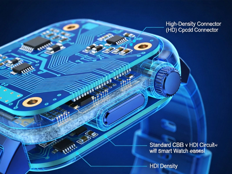
The Role of HDI Technology in Wearable Device MiniaturizationJuly/15/2026
Why IoT Sensors Rely on High-Density Interconnect TechnologyOctober/13/2026
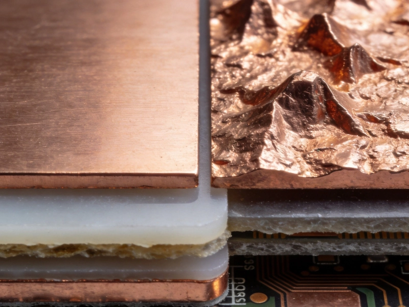
Understanding the Role of Copper Foil Roughness in Signal IntegritySeptember/23/2026
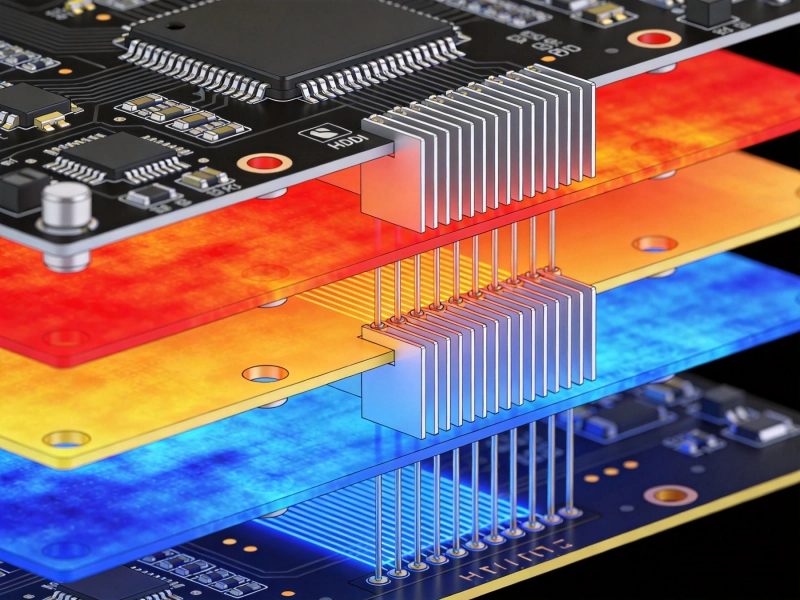
Effective Thermal Management Strategies for High-Density PCBsMay/28/2026
Managing Thermal Stress in Industrial Automation HDI BoardsOctober/19/2026