Open Nav

High-density Interconnect (HDI) designs enabling 5G communications, high-speed data centers, and advanced automotive radar require printed circuit boards that preserve Signal Integrity across demanding frequency ranges. Standard FR4 laminates, adequate for legacy applications, introduce excessive signal degradation that limits performance and constrains reach at elevated data rates. Low loss materials provide the electrical performance necessary for these advanced applications while maintaining the manufacturing compatibility HDI constructions demand. This article examines why low loss materials have become essential for high-speed HDI designs, exploring dielectric property fundamentals, material options, and design implications for engineers selecting laminates for next-generation products.
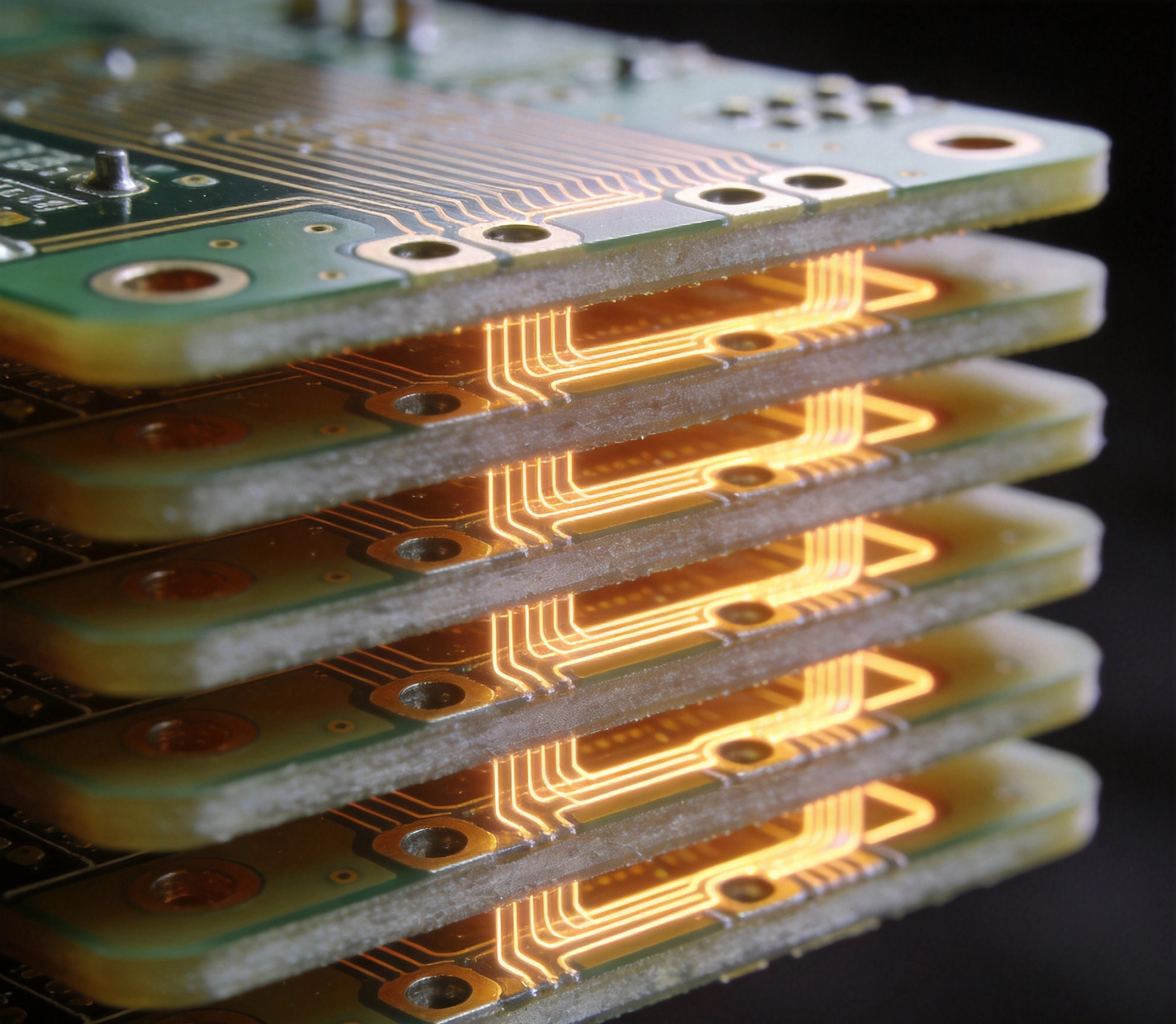
Signal attenuation in PCB traces arises from two primary loss mechanisms: conductor losses from trace resistance and dielectric losses from energy dissipation within substrate materials. While conductor losses dominate at lower frequencies, dielectric losses increasingly dominate as signal frequencies rise into the gigahertz range. This transition typically occurs between 1-5GHz depending on material properties, with dielectric contributions becoming dominant at frequencies where modern high-speed interfaces operate.
Dielectric loss derives from molecular interactions with alternating electric fields. Polar molecules attempt to follow field reversals, with lag between field and molecular response converting electrical energy to heat. The loss tangent (Df), also termed dissipation factor, quantifies this inefficiency. Materials with lower Df values dissipate less energy per signal cycle, preserving signal amplitude and waveform integrity throughout transmission paths. Standard FR4 exhibits Df values between 0.015-0.035, while advanced low loss materials achieve Df below 0.004—a ninefold improvement in dielectric efficiency.
The dielectric constant (Dk) determines signal propagation velocity and influences trace impedance calculations. Lower Dk values increase propagation velocity, reducing propagation delay in time-critical applications. More importantly, Dk stability across frequency and temperature ranges maintains consistent impedance—variations in Dk create impedance discontinuities that degrade signal quality. Low loss materials typically exhibit more stable Dk characteristics than standard substrates, providing both reduced loss and improved impedance consistency.
Modern high-speed serial interfaces transmit data at rates demanding attention to every loss mechanism. PCIe 4.0 operates at 16GT/s with 8GT/s and 32GT/s variants following rapidly. Ethernet systems now standard 25Gbps per lane with 56Gbps deployed and 112Gbps emerging. 5G millimeter-wave applications transmit at frequencies above 28GHz. Each generation increases bandwidth demands, pushing Signal Integrity requirements beyond capabilities of conventional Pcb Materials.
Insertion Loss budgets allocate total acceptable signal attenuation across channel components including connectors, traces, and vias. High-speed interfaces permit total Insertion Loss of 20-30dB at Nyquist frequencies, with stricter limits at higher data rates. Standard FR4 traces contribute 3-5dB loss per inch at 10GHz—losses that rapidly consume budgets in systems requiring multiple inches of routing. Low loss materials reduce trace contributions to 1-2dB per inch, preserving budget margin for connectors, cables, and manufacturing variations.
Skin Effect increasingly concentrates current density near conductor surfaces as frequencies rise, reducing effective cross-sectional area and increasing effective resistance. This phenomenon interacts with dielectric losses to produce combined effects that standard loss models inadequately predict. Advanced material characterization includes extraction of conductor-backed dielectric loss parameters that enable accurate simulation of combined loss mechanisms in high-speed designs.
HDI designs demand materials compatible with Sequential Lamination processes, fine-line patterning, and Microvia formation. Standard rigid laminates undergo thermal cycling during layer buildup, with multiple exposures to lamination temperatures exceeding 200°C. Materials must maintain stable electrical and mechanical properties through these thermal excursions without degradation that would compromise performance or reliability.
Thickness uniformity becomes critical as HDI constructions employ thinner dielectric layers than conventional multilayer boards. Signal layers in HDI designs commonly employ 50-100µm dielectric thicknesses compared to 150-300µm in standard multilayer constructions. These thinner dimensions demand materials with consistent resin content and glass weave distribution—variations that would produce larger percentage deviations in thinner layers. Low loss materials typically undergo more rigorous Quality Control than standard products, providing tighter thickness tolerances essential for HDI Impedance Control.
Microvia formation imposes additional material constraints. Laser Drilling, the standard method for creating HDI Microvias, requires specific resin characteristics that enable consistent ablation without residual smear or recast concerns. Standard FR4 resins work well with established laser parameters, while some advanced low loss materials require modified processing that may affect manufacturing yields. Material selection must balance electrical performance against manufacturing compatibility to achieve optimal cost-performance outcomes.
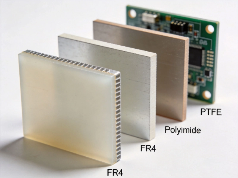
Hydrocarbon ceramic laminates represent the mainstream low loss category, combining moderate cost with excellent electrical performance. Rogers RO4000 series materials provide Df values of 0.002-0.004 with Dk of 3.4-6.15 depending on formulation. These materials process similarly to standard FR4, accepting standard drilling, plating, and lamination procedures that minimize manufacturing learning curves. The RO4003C variant, with Dk of 3.38 and Df of 0.0027, has become nearly ubiquitous in high-speed digital applications.
PTFE-based laminates offer the lowest loss characteristics available, with Df values below 0.002 and exceptional high-frequency stability. Rogers RT/duroid materials and Taconic TLC series serve applications demanding maximum performance regardless of cost. Processing challenges include Cte Mismatch with copper requiring specialized adhesive systems, dimensional instability requiring careful handling, and thermal characteristics that complicate mixed-technology assemblies with standard components.
Polyimide-based low loss materials balance performance with Hdi Manufacturing compatibility. Neutex and similar formulations provide Df values of 0.002-0.004 with processing characteristics approaching standard polyimide. These materials suit applications requiring the thermal stability and reliability of polyimide construction while benefiting from reduced dielectric loss. Aerospace and automotive applications particularly favor polyimide low loss options for their proven reliability heritage.
Data rate requirements establish baseline material selection. Designs operating below 5Gbps may adequately perform on standard FR4, though low loss materials improve margins even at lower frequencies. 5-10Gbps applications typically justify hydrocarbon ceramic materials that provide meaningful loss reduction without excessive cost premiums. Above 10Gbps, specialized low loss materials become essential, with PTFE options for the most demanding applications and hydrocarbon ceramics for cost-sensitive high-volume products.
Loss tangent specifications at target frequencies guide material comparison. Manufacturers specify Df at discrete frequencies—typically 1MHz, 10MHz, and sometimes 10GHz—enabling apples-to-apples comparison across material categories. Designers should select frequencies matching application requirements rather than relying on low-frequency specifications that may not predict high-frequency behavior accurately. Temperature-dependent Df variations matter for applications with wide thermal ranges, with automotive and outdoor deployments requiring particular attention to elevated-temperature loss characteristics.
Manufacturing compatibility assessments ensure selected materials integrate successfully with production processes. Consider drilling and plating requirements for through-holes, laser parameters for microvia formation, and lamination compatibility with other materials in hybrid stack-ups. Qualified fabricators with experience on specific materials provide valuable guidance during selection, often identifying materials that meet electrical requirements while minimizing manufacturing complications.
Hybrid stack-ups combining standard and low loss materials balance cost against performance within single board constructions. Critical high-speed signal layers receive low loss dielectrics while lower-frequency routing utilizes economical standard materials. This approach reduces material costs while ensuring optimal performance where it matters most—particularly valuable for board designs containing mixed signal types from high-speed serial links to power distribution networks.
Prepreg selection for hybrid constructions requires careful attention to thermal compatibility between material systems. Coefficient of thermal expansion (CTE) mismatches between adjacent layers create stress concentrations during thermal cycling that may compromise plated through-hole reliability. Low loss materials often exhibit different CTE values than standard prepregs, requiring attention to overall Stack-up Design that accommodates these differences through strategic layer positioning and thermal relief provisions.
Impedance budgeting allocates total loss across material systems when hybrid stack-ups distribute signals across standard and low loss routing layers. Designers should analyze loss contributions from each layer type, adjusting trace lengths and routing to ensure signal quality regardless of which material system carries specific signals. Design rule systems should specify different loss budgets for different layer types, preventing oversights that would route high-speed signals on unsuitable material layers.
Trace geometry optimization extracts maximum performance from low loss materials through careful attention to cross-sectional dimensions. Wider traces reduce conductor losses by increasing cross-sectional area, though impedance constraints limit practical width expansion. For controlled impedance designs, lower-Dk materials enable wider traces for equivalent impedance, directly reducing conductor losses while improving manufacturing yield by relaxing tolerance requirements.
Via optimization minimizes discontinuities that would negate material loss improvements. Through-hole stubs create resonant behavior at high frequencies, with stub lengths causing frequency-dependent loss peaks. Back-drilling removes unused barrel sections, with typical stub limits below 0.38mm (15mil) adequate for 10Gbps operation. Microvia constructions eliminate stubs entirely, with Sequential Lamination enabling direct capture pad connections that preserve signal integrity through layer transitions.
Reference plane design ensures return current paths complement low loss material investments. Broken or slotted reference planes create impedance discontinuities that introduce loss exceeding trace dielectric contributions. Solid reference planes adjacent to high-speed layers provide consistent impedance and minimize coupling to adjacent signal layers. When plane splits become necessary, stitching vias maintain return path continuity while preventing slot antenna effects that radiate interference.
Material characterization testing validates supplier specifications against actual board performance. Differential pair trace test vehicles enable extraction of Df and Dk values from impedance and loss measurements. Time-domain reflectometry characterizes impedance uniformity while frequency-domain measurements using vector network analyzers provide insertion loss data across operating frequency ranges. These measurements confirm that purchased materials perform as specified and that fabrication processes maintain material properties throughout production.
Process capability studies establish manufacturing tolerances for impedance-controlled designs on low loss materials. Impedance measurements across production panels characterize mean and variation, enabling statistical process capability indices that predict production yields. These studies identify systematic variations—panel edge effects, panel-to-panel differences, and systematic drift—that require process adjustments to achieve consistent high-speed performance.
Eye diagram testing provides end-to-end validation of channel performance including material loss contributions. Test setups inject high-speed patterns through representative channel configurations, measuring eye opening, jitter, and amplitude noise. Clear eye diagrams with adequate margins validate that material selections and design implementations meet interface specifications, providing confidence for production deployment.
Low loss materials command premiums of 2-10x compared to standard FR4, with pricing influenced by volume, performance level, and format. Sheet-based materials scale economically for larger board sizes, while panel-based pricing may favor particular form factors depending on fabricator capabilities. Overall cost impact depends on board size, layer count, and percentage of layers employing premium materials—hybrid stack-ups minimize material costs while maximizing performance where needed.
Manufacturing yield improvements on low loss materials partially offset material cost premiums. Tighter dielectric thickness tolerances reduce impedance variation, lowering scrap rates on impedance-controlled designs. More stable material properties simplify processing across thermal cycles, reducing delamination and other defect risks. These yield improvements prove particularly significant for complex HDI constructions where defect costs multiply through sequential processing.
System-level cost analysis may justify low loss material investments when accounting for extended reach, reduced equalization requirements, and improved signal margins. Channels built on low loss materials support longer trace lengths, enabling board designs that would require active repeaters or retimers on standard materials. Reduced equalization complexity simplifies SerDes implementation and reduces power consumption in high-speed links. Designers should evaluate total system costs rather than individual component expenses when justifying material investments.
Emerging applications at 100Gbps per lane and beyond demand continued material advancement beyond current low loss offerings. Ultra-low loss materials with Df below 0.001 target 112Gbps Ethernet and future high-speed serial standards. These materials employ novel filler systems and refined resin chemistries that push loss characteristics while maintaining manufacturing compatibility—though processing windows remain narrower than hydrocarbon ceramic alternatives.
Integrated passive materials enable embedded capacitors and resistors that reduce board size while improving high-frequency performance. These material systems embed passive functions within PCB constructions, eliminating parasitic inductances that compromise performance at high frequencies. Initial applications appear in RF modules where size reduction and performance improvement justify additional processing complexity.
Sustainability considerations increasingly influence material selection, with halogen-free and bio-based formulations emerging for environmentally conscious applications. These materials must achieve equivalent electrical performance to conventional products while meeting environmental standards increasingly demanded by regulations and customer requirements. Material suppliers continue developing formulations that balance electrical, environmental, and economic objectives.
Low loss materials have transitioned from optional enhancement to essential requirement for high-speed HDI designs operating above 5Gbps. The fundamental physics of dielectric loss impose performance limits that standard FR4 cannot overcome regardless of design optimization. Material selection directly determines achievable reach, power consumption, and margin for manufacturing variations—parameters that ultimately constrain product viability in demanding applications.
Successful high-speed HDI implementation requires balancing electrical performance against manufacturing compatibility and cost constraints. Hydrocarbon ceramic materials provide an effective middle ground for most applications, while PTFE options serve the most demanding requirements despite processing challenges. Hybrid stack-ups enable optimization that allocates premium materials where performance justifies costs while reserving standard materials for less critical functions.
As data rates continue escalating toward 100Gbps per lane and frequencies push into millimeter-wave ranges, material innovation remains essential for system advancement. Engineering teams selecting materials today must anticipate tomorrow's requirements, choosing platforms that enable technology evolution without requiring wholesale material changes. This long-term perspective, combined with rigorous validation of current implementations, positions products for success in rapidly advancing high-speed markets.
An Introduction to ABF (Ajinomoto Build-up Film) for Advanced HDIJuly/27/2026
Selecting the Right Dielectric Materials for High-Performance HDI PCBsJune/05/2026
Managing Layer-to-Layer Registration Accuracy in Multilayer HDIOctober/09/2026
Understanding the Role of Copper Foil Roughness in Signal IntegritySeptember/23/2026
What is High Density Interconnect (HDI) PCB?May/28/2026
Essential HDI PCB Design Rules for Beginners and ExpertsMay/28/2026
FR-4 vs. High-Tg Materials: What Works Best for HDI Applications?July/07/2026
Selecting the Right Dielectric Materials for High-Performance HDI PCBsMay/28/2026