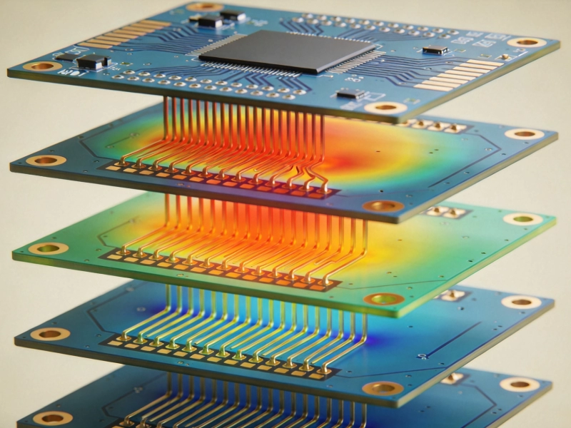
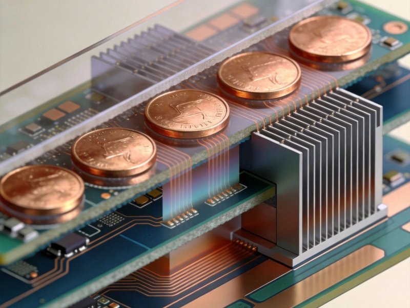
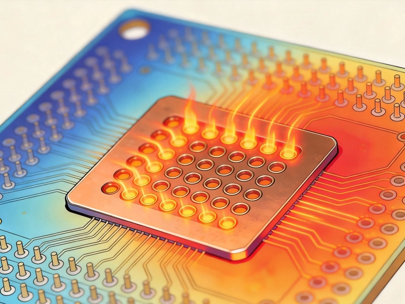
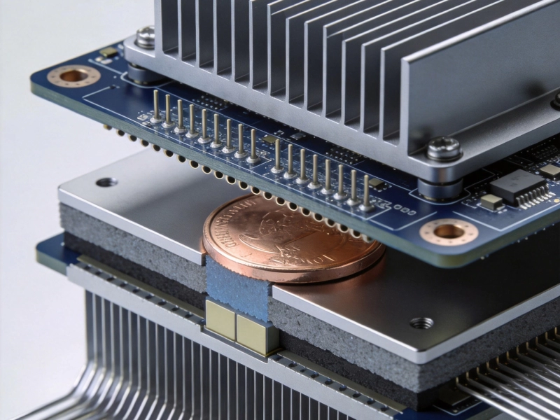
As electronic devices continue to shrink in size while increasing in functionality, the demand for High Density Interconnect (HDI) technology has never been greater. HDI PCBs represent the cutting edge of circuit board technology, enabling designers to pack more functionality into smaller spaces while improving electrical performance. Understanding the 6 types of HDI structures—from basic Type I to advanced Any-Layer (Type VI)—is essential for engineers and designers looking to maximize their design capabilities in today's compact electronic products.
Hdi Technology has revolutionized Electronics Manufacturing by introducing Microvias, blind and Buried Vias, and advanced lamination techniques that were unimaginable just a few decades ago. These innovations have enabled the development of smartphones, tablets, wearable devices, and countless other products that demand high component density in minimal space. However, with multiple HDI structure types available, choosing the right approach for your specific application requires careful consideration of cost, complexity, performance requirements, and manufacturability.
This comprehensive guide explores each of the six HDI structure types in detail, examining their characteristics, advantages, limitations, and typical applications. Whether you're designing the next generation of mobile devices or developing specialized industrial electronics, understanding these HDI structures will help you make informed decisions that optimize both performance and cost-effectiveness.

What is HDI Technology?
Before diving into the specific structure types, it's important to understand what makes Hdi Technology unique and why it has become so critical in modern Electronics Design.
Core HDI Characteristics
HDI technology is defined by several key characteristics that distinguish it from traditional Pcb Manufacturing:
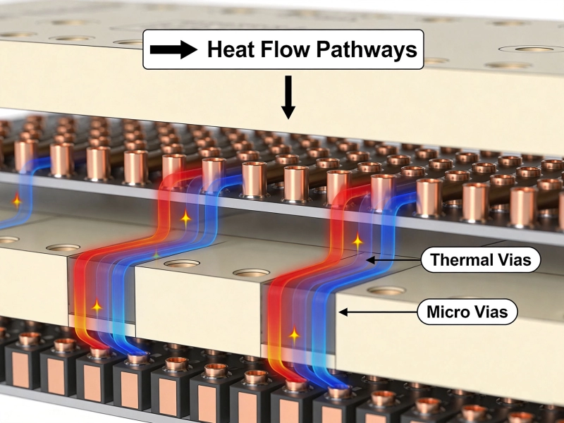
- Microvias: Small vias typically less than 150 microns (6 mils) in diameter, compared to traditional vias that are 200-300 microns or larger. Microvias enable closer component spacing and higher routing density.
- Blind and Buried Vias: Unlike traditional through-hole vias that extend through the entire board, Blind Vias connect an outer layer to one or more inner layers without passing through the entire board, while buried vias connect only inner layers without reaching the surface.
- Capture pads: Smaller landing pads for microvias that further increase routing density and allow closer component placement.
- Sequential Lamination: Multiple lamination cycles that build up the board layer by layer, enabling complex via structures that wouldn't be possible with single lamination.
- Finer lines and spaces: HDI processes support trace and space widths as small as 75 microns (3 mils) or less, compared to 100-150 microns for standard processes.
- Higher layer counts: HDI technology enables efficient use of 10+ layers in compact form factors, where traditional designs might require much larger boards or more layers to achieve the same functionality.
Why HDI Matters in Modern Electronics
The importance of HDI technology stems from several industry trends that continue to drive demand for higher density:
- Miniaturization: Consumer electronics continue to shrink while adding features, requiring higher component density in smaller footprints.
- Performance requirements: Higher speed signals and more complex functionality require better Signal Integrity and more routing channels, both enabled by HDI.
- Component packaging: Advanced packaging like BGA, QFN, and chip-scale packages with finer pitch require the routing density that only HDI can provide.
- Cost optimization: While Hdi Boards cost more per square inch, they often reduce overall system cost by enabling smaller form factors, fewer boards, and simplified assembly.
- Reliability improvements: Shorter interconnects and better Signal Integrity can improve overall system reliability despite increased complexity.
Type I HDI: The Foundation of High Density
Type I HDI represents the entry point into High-density Interconnect technology, offering significant improvements over traditional through-hole via designs while maintaining relative manufacturing simplicity.
Type I Structure Definition
Type I HDI features:
- Single-side microvias: Microvias that extend from one outer layer to the first inner layer only
- Through-hole vias: Traditional through-hole vias for inter-layer connections that span the entire board thickness
- No buried vias: All vias either start or end on an outer layer
- Single lamination cycle: Manufactured in a single lamination process, similar to traditional multilayer boards
This structure represents the simplest form of HDI, incorporating microvias on one side of the board while maintaining traditional through-hole vias for most inter-layer connections. The microvias typically have diameters of 100-150 microns, compared to 200-300 microns for traditional vias.
Advantages of Type I HDI
Type I HDI offers several compelling benefits:
- Cost-effective: Lower cost than more complex HDI types due to simpler manufacturing process
- Higher component density: Microvias enable closer component spacing on the Microvia side
- Improved signal integrity: Shorter via stubs reduce signal reflections and improve high-frequency performance
- Better Thermal Performance: More efficient Heat Dissipation through smaller vias
- Manufacturing familiarity: Builds on existing processes with minimal added complexity
Limitations and Considerations
Despite its advantages, Type I HDI has limitations:
- Asymmetric routing: High density is only achieved on one side of the board
- Via stubs: Through-hole vias still have stubs that can affect signal integrity in high-speed applications
- Limited density improvement: Density gains are modest compared to more advanced HDI types
- Layer efficiency: Through-hole vias consume routing channels on all layers they pass through
Typical Applications
Type I HDI is well-suited for:
- Mid-range consumer electronics: Where some density improvement is needed but cost sensitivity remains high
- Industrial controls: Applications requiring improved reliability and signal performance
- Automotive Electronics: Where space savings are valuable but extreme density isn't required
- Medical devices: Applications benefitting from improved signal integrity without extreme Miniaturization
Type II HDI: Double-Sided Microvias
Type II HDI builds upon Type I by adding microvias to both sides of the board, significantly increasing routing density and design flexibility.
Type II Structure Definition
Type II HDI features:
- Double-sided microvias: Microvias on both outer layers connecting to the first inner layer
- Through-hole vias: Traditional through-hole vias for connections between deeper layers
- No buried vias: All vias still connect to at least one outer layer
- Single lamination cycle: Still manufactured in a single lamination process
This symmetric approach provides high-density routing capabilities on both sides of the board, making it ideal for designs with components on both surfaces and balanced routing requirements.
Advantages of Type II HDI
Type II HDI offers enhanced capabilities:
- Balanced density: High routing density available on both board surfaces
- Design flexibility: Components can be placed on both sides with optimal routing
- Improved Thermal Performance: Thermal Vias can be placed on both sides for better Heat Dissipation
- Signal routing options: More routing channels available for complex designs
- Cost-effective density: Significant density improvement without Sequential Lamination costs
Design Considerations
When implementing Type II HDI, consider:
- Layer balancing: Ensure balanced copper distribution to prevent warpage
- Via placement: Careful planning of Microvia and through-hole via locations
- Thermal Management: Leverage double-sided Thermal Vias for improved heat dissipation
- Cost vs. benefit: Evaluate whether the additional microvias justify the cost increase over Type I
Typical Applications
Type II HDI excels in:
- Smartphones and tablets: Where balanced density on both sides is essential
- Portable electronics: Applications with components on both surfaces
- Communication devices: Complex RF and digital circuitry requiring high density
- Advanced consumer electronics: Products demanding significant miniaturization
Type III HDI: Introduction of Buried Vias
Type III HDI represents a significant advancement by introducing buried vias, enabling true three-dimensional interconnection and dramatically improving routing efficiency.
Type III Structure Definition
Type III HDI features:
- Double-sided microvias: Microvias on both outer layers connecting to adjacent inner layers
- Buried vias: Vias that connect inner layers without reaching either surface
- Through-hole vias: Limited use of through-hole vias for specific applications
- Sequential lamination: Requires multiple lamination cycles to create Buried Via structures
This structure enables complex three-dimensional routing where signals can move between layers without consuming surface area or creating via stubs on outer layers.
Advantages of Type III HDI
Type III HDI provides substantial benefits:
- Maximum routing density: Buried vias free surface area for components and routing
- Improved signal integrity: Elimination of via stubs reduces signal reflections
- Layer efficiency: Inner layers can be used more efficiently for routing
- Complex interconnection: Enables sophisticated three-dimensional routing schemes
- Reduced board size: Higher density enables smaller board footprints
Manufacturing Complexity
Type III HDI introduces manufacturing challenges:
- Sequential lamination: Multiple lamination cycles increase process time and cost
- Alignment requirements: Precise alignment required between lamination cycles
- Yield considerations: More process steps can impact overall yield
- Design rules: More complex design rules and constraints
Typical Applications
Type III HDI is essential for:
- High-end smartphones: Where maximum density in minimum space is required
- Wearable devices: Extremely space-constrained applications
- Advanced medical devices: Complex electronics in miniature form factors
- Military and aerospace: High-performance applications with size constraints
Type IV HDI: Enhanced Buried Via Structures
Type IV HDI builds upon Type III by incorporating more complex Buried Via structures and typically higher layer counts, pushing the boundaries of density and performance.
Type IV Structure Definition
Type IV HDI features:
- Multiple buried via layers: Buried vias connecting multiple inner layer pairs
- Complex via stacks: Stacked Microvias and buried vias for vertical interconnection
- Higher layer counts: Typically 10+ layers to maximize routing density
- Advanced sequential lamination: Multiple precise lamination cycles
This structure enables extremely dense designs with sophisticated interconnection schemes that maximize the use of all available layers.
Advantages of Type IV HDI
Type IV HDI delivers exceptional capabilities:
- Ultimate density: Maximum component and routing density achievable
- Complex signal routing: Supports highly complex routing schemes
- Power distribution: Excellent power and ground distribution through multiple layers
- Signal integrity: Optimized for high-speed and high-frequency applications
- Miniaturization: Enables the most compact designs possible
Design and Manufacturing Challenges
Type IV HDI presents significant challenges:
- Extreme complexity: Requires sophisticated design tools and expertise
- Higher cost: Multiple lamination cycles and complex processing increase cost
- Yield management: More process steps require careful yield optimization
- Thermal Management: High component density requires advanced thermal solutions
Typical Applications
Type IV HDI is used in:
- Flagship smartphones: Leading-edge mobile devices with maximum functionality
- Advanced computing: High-performance computing in compact form factors
- Sophisticated IoT devices: Complex edge computing devices
- Military applications: Mission-critical Systems with extreme requirements
Type V HDI: Alternate Layer Structures
Type V HDI introduces alternate layer structures where different layers have different via configurations, optimizing the board for specific performance and cost requirements.
Type V Structure Definition
Type V HDI features:
- Asymmetric via structures: Different via configurations on different layer pairs
- Optimized layer usage: Layers optimized for specific functions (power, signal, ground)
- Targeted HDI: HDI features applied where needed most
- Cost optimization: Balances HDI benefits with manufacturing cost
This approach allows designers to apply HDI technology strategically, using the most cost-effective structure for each area of the board.
Advantages of Type V HDI
Type V HDI offers targeted benefits:
- Cost optimization: Applies HDI only where it provides maximum benefit
- Performance optimization: Optimizes different areas for different requirements
- Design flexibility: Enables hybrid approaches for complex requirements
- Manufacturing efficiency: Reduces unnecessary complexity in non-critical areas
Design Considerations
When implementing Type V HDI, consider:
- Area partitioning: Identify areas that benefit most from HDI features
- Interface management: Manage transitions between different structure types
- Cost-benefit analysis: Carefully evaluate HDI application in each area
- Design complexity: Manage increased design complexity from mixed structures
Typical Applications
Type V HDI suits:
- Mixed-signal designs: Where different areas have different requirements
- Cost-sensitive high-performance: Applications balancing performance and cost
- Complex systems: Designs with varied requirements across the board
- Optimized solutions: Applications where targeted optimization provides maximum value
Type VI HDI: Any-Layer HDI
Type VI, also known as Any-layer Hdi, represents the pinnacle of HDI technology, enabling microvias on any layer of the board and providing maximum design flexibility and density.
Any-Layer Structure Definition
Type VI HDI features:
- Microvias on any layer: Microvias can connect any adjacent layer pair
- Complete flexibility: No restrictions on via placement based on layer
- Maximum density: Ultimate routing and component density
- Complex stacking: Sophisticated via stacking and skipping capabilities
This revolutionary approach removes virtually all restrictions on via placement, enabling designers to optimize routing and component placement without traditional constraints.
Advantages of Any-Layer HDI
Type VI HDI delivers unmatched capabilities:
- Ultimate flexibility: Complete design freedom for via placement
- Maximum density: Highest possible component and routing density
- Optimized performance: Signal routing optimized without constraints
- Smallest form factors: Enables the most compact designs
- Advanced applications: Supports the most demanding electronic applications
Challenges and Considerations
Any-layer Hdi presents significant challenges:
- Extreme cost: Highest manufacturing cost among all HDI types
- Complex manufacturing: Most complex HDI structure to manufacture
- Design expertise: Requires extensive HDI design experience
- Yield challenges: Multiple process steps impact yield
Typical Applications
Any-Layer HDI is reserved for:
- Leading-edge smartphones: Flagship devices with maximum requirements
- Advanced Wearables: Ultra-compact sophisticated devices
- High-performance computing: Applications where size and performance are critical
- Military and aerospace: Mission-critical applications with extreme requirements
Selecting the Right HDI Type for Your Application
Choosing the appropriate HDI structure type requires careful consideration of multiple factors beyond just density requirements.
Key Selection Criteria
Consider these factors when selecting an HDI type:
- Component density requirements: How many components need to fit in the available space?
- Routing complexity: How complex are the interconnection requirements?
- Signal integrity requirements: What are the speed and frequency requirements?
- Thermal management needs: How much heat dissipation is required?
- Cost constraints: What is the target cost for the PCB?
- Manufacturing capabilities: What HDI types can your manufacturer reliably produce?
- Reliability requirements: What are the reliability and lifecycle requirements?
Cost vs. Performance Trade-offs
Understanding the cost-performance relationship:
- Type I-II: Best cost-performance ratio for moderate density improvements
- Type III: Good balance of density and cost for high-density applications
- Type IV-VI: Premium cost for maximum density and performance
Design-for-Manufacturability Considerations
Ensure your design is manufacturable:
- Manufacturer capabilities: Verify your chosen manufacturer can produce the selected HDI type
- Design rules: Follow manufacturer-specific design rules for the HDI type
- Yield optimization: Design for yield by respecting manufacturing constraints
- Testing requirements: Plan for appropriate testing of complex HDI structures
Emerging Trends in HDI Technology
HDI technology continues to evolve, with new trends shaping the future of high-density interconnects.
Advanced Materials
New materials enable better HDI performance:
- Ultra-thin dielectrics: Materials as thin as 25 microns for thinner boards
- Low-loss Materials: Improved high-frequency performance
- High-TG materials: Better thermal performance for high-power applications
Smaller Via Technologies
Vias continue to shrink:
- Sub-50 micron vias: Emerging capabilities for ultra-fine pitch
- Laser-drilled microvias: Improved precision and smaller sizes
- Copper-filled vias: Better thermal and electrical performance
Integration with Advanced Packaging
HDI integrates with new packaging technologies:
- System-in-Package: Hdi Boards combined with SiP for maximum density
- Embedded components: Components embedded within HDI layers
- 2.5D/3D packaging: HDI supporting advanced multi-chip modules
Conclusion
The six types of HDI structures—from Type I to Any-Layer—represent a spectrum of capabilities that enable designers to meet increasingly demanding requirements for electronics miniaturization and performance. Understanding each type's characteristics, advantages, and limitations is essential for making informed decisions that balance performance, cost, and manufacturability.
As electronic devices continue to evolve, HDI technology will remain at the forefront of enabling innovation. The key to success lies not just in selecting the most advanced HDI type, but in choosing the right HDI type for your specific application requirements. By carefully considering your needs in terms of density, performance, cost, and manufacturability, you can leverage HDI technology to create products that meet today's demanding market requirements while positioning yourself for future innovations.
Whether you're implementing basic Type I HDI for cost-sensitive applications or pushing the boundaries with Any-Layer HDI for cutting-edge products, understanding these six structure types provides the foundation for making informed design decisions that optimize both technical performance and business success.
Frequently Asked Questions
Q: What is the main difference between Type I and Type II HDI?
A: The primary difference is that Type I has microvias on only one side of the board, while Type II has microvias on both sides. Type II provides balanced high-density routing on both surfaces, while Type I concentrates high density on one side only.
Q: When should I choose Type III HDI over Type II?
A: Choose Type III when you need maximum routing density and improved signal integrity through elimination of via stubs. Type III's buried vias free up surface area and provide better layer utilization, justifying the additional cost of sequential lamination.
Q: Is Any-Layer HDI worth the additional cost for most applications?
A: No, Any-Layer HDI is typically only justified for the most demanding applications where maximum density and design flexibility are critical. For most applications, Type III or Type IV HDI provides a better balance of performance and cost.
Q: How does layer count affect HDI structure selection?
A: Higher layer counts generally benefit from more advanced HDI types (III-VI) because they provide more efficient interconnection between layers. Lower layer counts (4-6 layers) can often be served well by Type I or Type II HDI.
Q: Can I mix different HDI types on the same board?
A: Yes, Type V HDI specifically allows mixing different HDI structures on different areas of the same board. This approach can optimize cost by applying advanced HDI only where needed most.