
High Density Interconnect boards, commonly called Hdi Boards, represent the pinnacle of PCB Miniaturization. With Microvias smaller than a human hair and ball grid array packages hiding hundreds of solder joints beneath a component the size of a fingernail, these boards push manufacturing tolerances to the limit. The challenge is that many of the most critical connections in an HDI design are completely invisible to the naked eye and even to standard automated optical inspection. They are buried inside the package, hidden under component bodies, or located in layers that cannot be accessed without destroying the board.
This is where X-ray Inspection becomes essential. Automated X-ray Inspection, or AXI, uses ionizing radiation to penetrate board materials and reveal internal structures that would otherwise be impossible to examine. For Hdi Boards with their high component density and complex multi-layer architectures, AXI is not merely an additional quality check. It is often the only way to verify that hidden connections meet reliability standards.
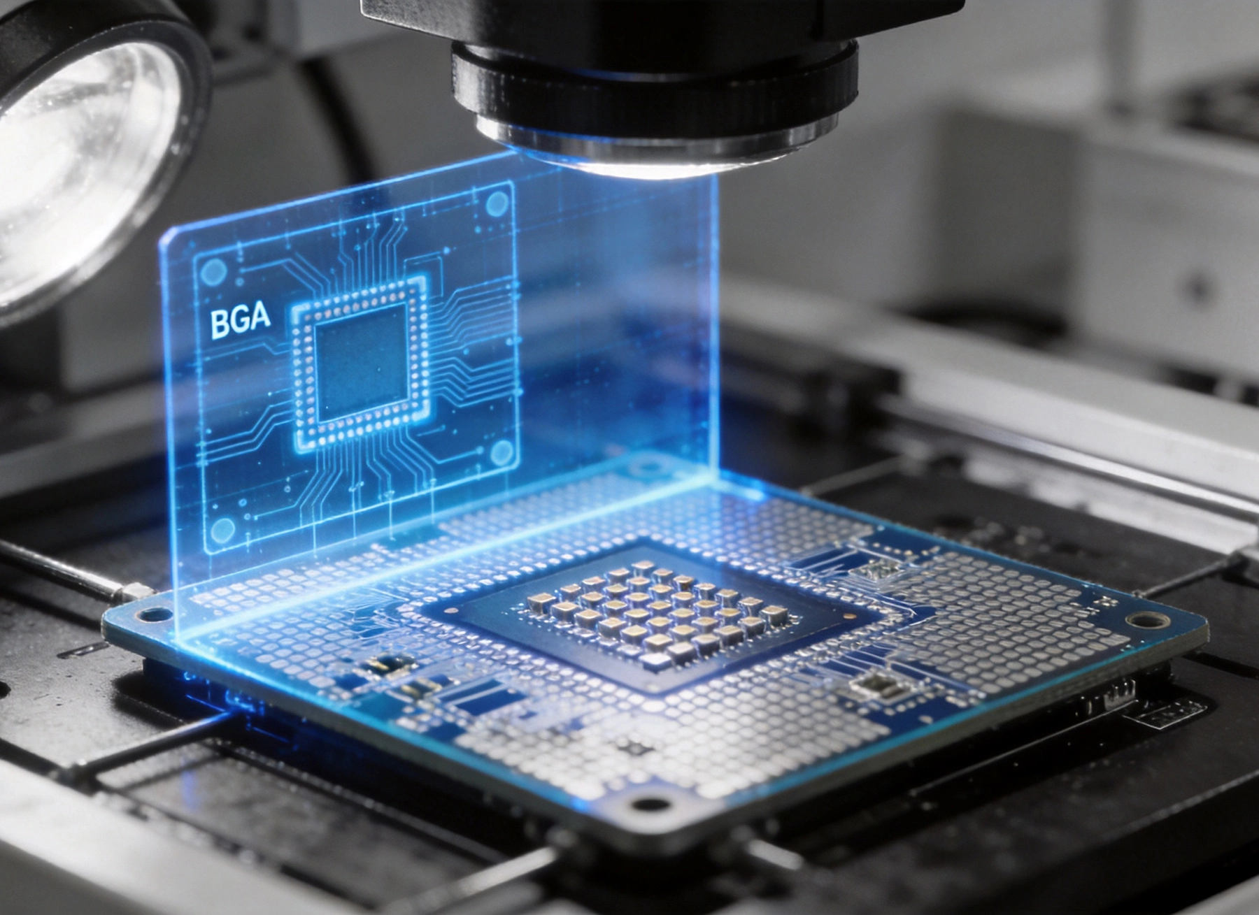
Hdi Technology employs Microvias, typically defined as vias with diameters below 150 microns, to achieve higher routing density than conventional multilayer boards. These microvias are often laser-drilled and can be stacked or staggered between layers. The density of interconnection points in an HDI board is orders of magnitude greater than in standard PCB designs.
The components mounted on HDI boards compound the inspection challenge. Ball grid arrays, or BGAs, have solder joints arranged in a grid pattern underneath the package body. The package itself blocks any optical view of the joints. Quad flat no-lead packages, or QFNs, similarly hide their bottom-side terminations. With packages like these making up the majority of components on a typical HDI board, the majority of solder joints are simply not accessible to visual inspection.
Conventional through-hole inspection methods like flying probe testing have limited effectiveness on HDI boards because access to internal nodes is restricted. The only way to see what is happening inside these structures is to use a technique that can see through the materials that surround the joints.
X-rays are a form of electromagnetic radiation with wavelengths much shorter than visible light. This short wavelength allows X-rays to penetrate most non-metallic materials, including the epoxy resins and fiberglass that make up PCB substrates. Different materials absorb X-rays to different degrees depending on their atomic density. Heavier elements like lead and tin absorb more X-rays than lighter elements like carbon and oxygen.
This differential absorption is what makes X-ray imaging useful. Copper traces and solder joints, which contain heavier elements, appear darker or brighter in an X-ray image depending on the imaging mode. The surrounding board material, made primarily of light elements, appears more transparent. By capturing the pattern of absorption and transmission, X-ray systems can create images that reveal internal structure.
Simple 2D X-ray radiography projects the entire board thickness onto a single image plane. While this can reveal gross defects, it suffers from overlapping information. Features at different depths within the board stack up on top of each other, making it difficult or impossible to isolate specific joints. 2D imaging is useful for finding gross defects like missing components or large voids, but lacks the resolution needed for detailed solder joint analysis.
Computed tomography, or CT scanning, creates true 3D images by rotating the board and collecting thousands of 2D projections from different angles. Sophisticated algorithms reconstruct these projections into a volumetric dataset that can be sliced at any depth or angle. CT imaging provides the ultimate in inspection capability, but the time required for scanning and reconstruction makes it unsuitable for high-volume production inspection.
Real-time radiography systems use continuous X-ray imaging with digital detectors that update at video frame rates. This allows inspectors to manipulate the board and view structures from different angles without stopping to collect new images. Real-time systems are faster than CT but still require manual interpretation.
Laminography is a technique that images a specific plane within an object while blurring structures above and below that plane. This is particularly useful for HDI boards because it can isolate individual layer interfaces within the multilayer stack. By focusing on specific layers, laminography can reveal defects that would be obscured in conventional 2D radiography.
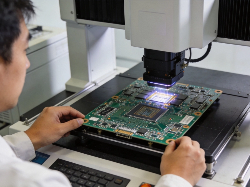
Modern AXI systems consist of an X-ray source, a precision manipulator or conveyor system, a digital X-ray detector, and automated image analysis software. The X-ray source is typically a microfocus tube that can produce spot sizes small enough to resolve fine features. Higher magnification requires smaller spot sizes, but this also reduces the available X-ray intensity.
Digital detectors convert X-ray photons into electronic signals that form the image. Direct detectors use semiconductor materials that directly convert X-ray photons. Indirect detectors first convert X-rays to visible light using a scintillator and then image the light with optical sensors. Both technologies offer sufficient resolution for HDI inspection when properly configured.
The power of modern AXI systems lies in their automated image analysis capabilities. Rather than relying on human operators to examine every image, the system automatically compares captured images against known-good reference patterns. Machine vision algorithms detect variations in solder joint appearance that indicate defects.
Advanced systems use machine learning to improve defect detection accuracy over time. By training on samples of known defects, these systems learn to identify subtle patterns that might be missed by rule-based algorithms. This capability is particularly valuable for HDI boards where defect modes can be complex and varied.
Voids are gas pockets trapped within solder joints during the reflow process. Small voids are normal and generally acceptable, but excessive voiding weakens joints and can lead to crack propagation under thermal or mechanical stress. In BGA packages, voids are particularly concerning because the solder joint is the only mechanical connection between the component and the board.
X-ray imaging reveals voids as darker spots or regions within the brighter solder joint. The size, location, and percentage of voiding relative to total joint area can be measured from X-ray images. Industry standards like IPC-A-610 specify maximum acceptable void percentages for different applications, and AXI systems can automatically flag joints that exceed these thresholds.
Bridging occurs when solder connects two adjacent pads that should remain isolated. On fine-pitch components, bridges might be too small to see optically even if the component body did not block the view. Under BGAs, bridges are completely invisible to any optical inspection method.
X-ray imaging makes bridging immediately apparent. A bridge appears as a connecting region of solder between two adjacent joints, visible from the top-down view as a widened region that spans between what should be separate pads. AXI systems can be programmed to detect bridging by identifying any solder connection between adjacent joints.
The head-in-pillow defect occurs when a BGA solder ball partially reflows and forms a weak connection with the pad, but does not fully coalesce into a proper solder joint. This creates an intermittent connection that might pass electrical testing but fails under vibration or thermal cycling. Head-in-pillow is notoriously difficult to detect because the joint often appears mostly intact in optical inspection and the electrical connection might be intermittent.
X-ray imaging reveals head-in-pillow as a characteristic appearance where the solder ball retains some of its original spherical shape rather than spreading completely flat onto the pad. The joint might show a visible gap or irregular interface between ball and pad. While definitive detection requires careful image interpretation, experienced inspectors can identify this defect pattern reliably in X-ray images.
Components that are not properly centered on their pads create reliability risks even when solder joints appear to have formed. A BGA that is shifted by even a few mils might have some balls that are only partially landed on their pads, creating weak joints that are prone to failure. In severe misalignment, balls might land entirely off their pads.
X-ray imaging reveals component position relative to pad patterns clearly. For BGAs, the pattern of solder balls relative to the underlying pad array indicates any positional offset. AXI systems can automatically calculate offsets and flag components that are misaligned beyond acceptable tolerances.
A BGA with missing solder balls creates open circuits that are completely invisible to optical inspection under the package body. Even looking at the package from an angle often cannot reveal whether all balls are present. X-ray imaging shows the complete ball array and clearly indicates any missing positions.
Missing balls can occur due to handling damage, improper printing of solder paste, or ball detachment during assembly. Whatever the cause, AXI inspection catches these defects reliably because every ball position is visible in the image regardless of package overhang.
Cracks in solder joints can develop during thermal cycling or mechanical stress. These cracks might not be visible optically because they run through the bulk of the joint rather than across its surface. A crack that is invisible to AOI might still cause intermittent electrical failures in the field.
While cracks are difficult to detect in production inspection, high-resolution X-ray imaging can sometimes reveal cracks as dark lines within the solder joint. CT imaging is particularly effective for crack detection because it can examine the joint from multiple angles and reconstruct its internal structure. For critical applications, computed tomography provides the best chance of detecting subtle cracks.
AXI is typically positioned after reflow soldering but before final test. Some manufacturers use AXI as a sampling tool, inspecting a statistical sample of boards rather than one hundred percent. Others use it for one hundred percent inspection of critical assemblies where defect escape costs are high.
For HDI boards with BGA and QFN components, one hundred percent AXI inspection is often justified by the difficulty of rework and the cost of field failures. Automotive, aerospace, and Medical Electronics manufacturers commonly require AXI inspection as part of their quality assurance programs.
AXI does not replace optical inspection but complements it. AOI catches many defects including component polarity errors, missing components, tombstoning, and gross solder issues. AXI then inspects the joints that AOI cannot see. Together, these methods provide more comprehensive coverage than either alone.
Electrical testing, including in-circuit test and functional test, provides another layer of verification. A board that passes electrical test might still have marginal defects that will fail prematurely in the field. AXI catches structural defects that do not cause immediate electrical failure but create reliability risks. The combination of AOI, AXI, and electrical testing provides the most robust quality assurance.
While X-ray can reveal internal structures, the achievable resolution is limited by X-ray physics. Very small features like Microvia barrel walls and fine-pitch BGA balls approach the limits of what even high-performance systems can resolve. For the smallest features in modern HDI boards, electron microscopy or cross-sectional analysis might be necessary for detailed examination.
Some materials are nearly invisible to X-ray inspection. Vias filled with conductive paste rather than Copper Plating can be difficult to distinguish from unfilled vias. Components with heavy metal enclosures block X-rays and prevent inspection of joints underneath. High-density ceramic capacitors might appear opaque in X-ray images, obscuring any joints beneath them.
Some defects require experienced operators to interpret correctly. The appearance of voids can be confused with other internal features. Head-in-pillow defects might be subtle and easily missed. Defects that are obvious in retrospect can be missed by inspectors who are not specifically looking for them. Training and procedure discipline are essential for reliable AXI inspection.
Not every PCB manufacturer has AXI capability in-house. For those who need external inspection services, choosing the right provider matters. Look for providers with experience inspecting your specific component types and board technologies. Ask about their resolution capabilities, inspection throughput, and defect detection rates.
Request sample inspection reports that demonstrate the quality of their analysis. A professional AXI service should provide detailed defect classification, image documentation, and clear recommendations for disposition. Avoid providers who offer only pass-fail results without supporting evidence.
X-ray inspection has become indispensable for HDI board quality assurance. The hidden defects that optical inspection cannot reach are exactly the defects that AXI excels at finding. Voids, bridges, head-in-pillow, misalignment, and missing balls are all reliably detected with proper X-ray imaging.
As Hdi Technology continues to advance, with ever-smaller features and higher densities, the importance of X-ray inspection will only increase. The investment in AXI capability, whether in-house or through qualified service providers, pays dividends in reduced field failures, improved customer satisfaction, and lower total cost of quality.
For manufacturers committed to producing reliable HDI assemblies, AXI is not optional. It is a fundamental requirement for understanding what is really inside the boards you build.
No. While X-ray inspection detects many defects, it has limitations. Micro-cracks that run parallel to the X-ray beam might not be visible. Some defect types require cross-sectional analysis or electron microscopy for definitive detection. AXI is most effective for gross structural defects like voids, bridges, and alignment issues.
AXI typically refers to 2D or real-time 3D X-ray imaging used for production inspection. Computed tomography is a specific technique that creates true volumetric images by rotating the sample and reconstructing many projections. CT provides superior detail for complex analysis but is slower and more expensive than conventional AXI.
Inspection time varies by board complexity and whether inspection is manual or automated. A simple automated scan might take a few minutes per board. Detailed inspection of complex HDI boards with many BGA components can take fifteen minutes or more. CT scans for critical failure analysis can take an hour or longer.
Yes. The X-ray dose used for inspection is low enough that it does not cause any damage or degradation to electronic components or boards. The radiation exposure is confined to the inspection system and does not leave residual radioactivity.
For critical applications in automotive, medical, aerospace, and other high-reliability sectors, one hundred percent inspection is common. For consumer electronics, statistical sampling based on defect risk and cost of failure might be appropriate. Work with your quality engineer to determine the appropriate inspection level for your specific application.
How to Implement Effective Impedance Control in HDI DesignsJuly/28/2026

Overcoming the Challenges of Testing Fine-Pitch BGA on HDISeptember/04/2026
Advanced Testing Methods for High-Density Interconnect PCBsMay/28/2026
Flying Probe vs. Fixture Testing: Which is Best for HDI PCBs?June/11/2026
The Art of Microvia Placement: Staggered vs. Stacked ViasSeptember/24/2026
Non-Destructive Testing Techniques for Multilayer HDI PCBsSeptember/29/2026
The Importance of Electrical Testing for Microvia ReliabilityJuly/09/2026

Mastering Stack-up Design for Optimal HDI PerformanceJune/08/2026